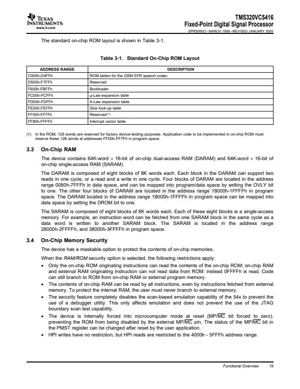
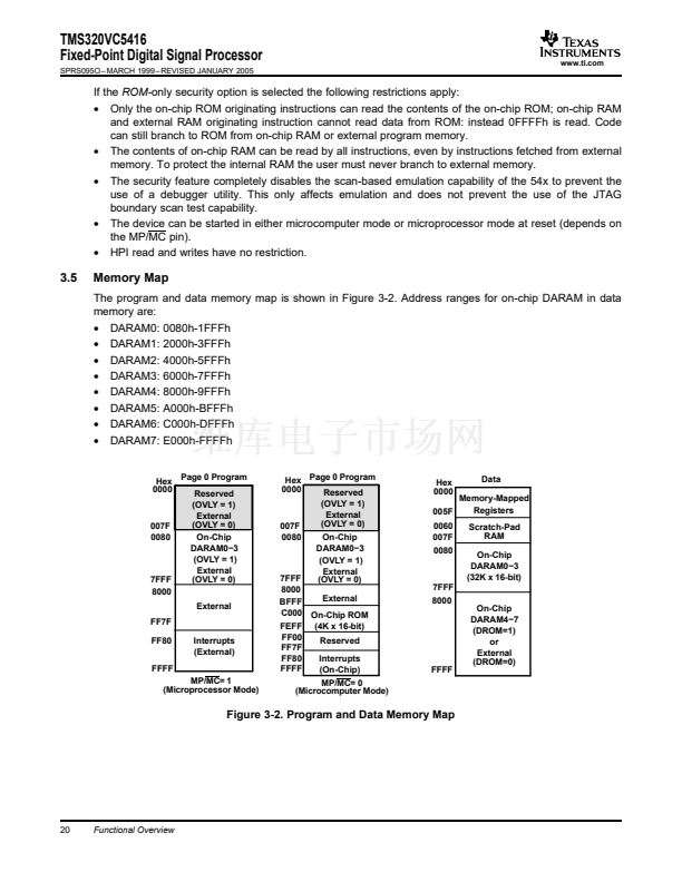
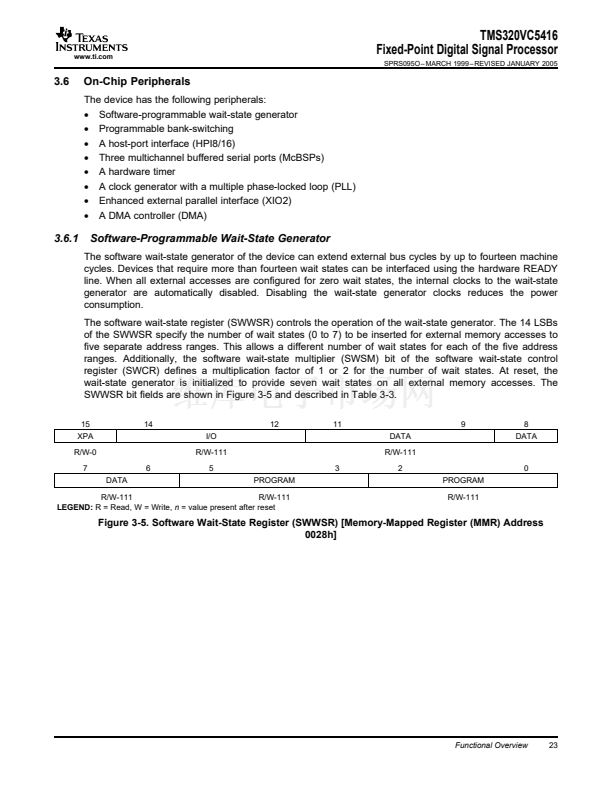
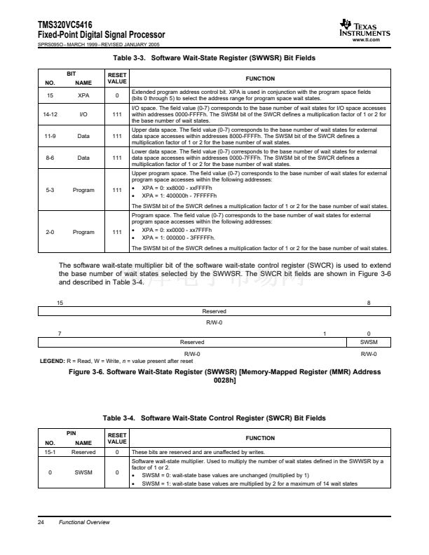
TMS320VC5416
Fixed-Point Digital Signal Processor
SPRS095O 鈥?MARCH 1999 鈥?REVISED JANUARY 2005
www.ti.com
Table 2-2. Signal Descriptions (continued)
TERMINAL
NAME
READY
I/O
(1)
DESCRIPTION
Data ready. READY indicates that an external device is prepared for a bus transaction to be completed. If the
device is not ready (READY is low), the processor waits one cycle and checks READY again. Note that the
processor performs ready detection if at least two software wait states are programmed. The READY signal is
not sampled until the completion of the software wait states.
Read/write signal. R/W indicates transfer direction during communication to an external device. R/W is normally
in the read mode (high), unless it is asserted low when the DSP performs a write operation. R/W is placed in the
high-impedance state in the hold mode; and it also goes into the high-impedance state when OFF is low.
I/O strobe signal. IOSTRB is always high unless low-level asserted to indicate an external bus access to an I/O
device. IOSTRB is placed in the high-impedance state in the hold mode; it also goes into the high-impedance
state when OFF is low.
Hold input. HOLD is asserted to request control of the address, data, and control lines. When acknowledged by
the device, these lines go into the high-impedance state.
Hold acknowledge. HOLDA indicates to the external circuitry that the processor is in a hold state and that the
address, data, and control lines are in the high-impedance state, allowing them to be available to the external
circuitry. HOLDA also goes into the high-impedance state when OFF is low. Figure 2-2 This pin is driven high
during reset.
Microstate complete. MSC indicates completion of all software wait states. When two or more software wait
states are enabled, the MSC pin goes active at the beginning of the first software wait state and goes inactive
high at the beginning of the last software wait state. If connected to the READY input, MSC forces one external
wait state after the last internal wait state is completed. MSC also goes into the high-impedance state when OFF
is low.
Instruction acquisition signal. IAQ is asserted (active low) when there is an instruction address on the address
bus and goes into the high-impedance state when OFF is low.
TIMER SIGNALS
CLKOUT
CLKMD1
(2)
CLKMD2
(2)
CLKMD3
(2)
X2/CLKIN
(2)
X1
TOUT
O/Z
Clock output signal. CLKOUT can represent the machine-cycle rate of the CPU divided by 1, 2, 3, or 4 as
configured in the bank-switching control register (BSCR). Following reset, CLKOUT represents the ma-
chine-cycle rate divided by 4.
Clock mode select signals. CLKMD1-CLKMD3 allow the selection and configuration of different clock modes
such as crystal, external clock, and PLL mode. The external CLKMD1-CLKMD3 pins are sampled to determine
the desired clock generation mode while RS is low. Following reset, the clock generation mode can be
reconfigured by writing to the internal clock mode register in software.
Clock/oscillator input. If the internal oscillator is not being used, X2/CLKIN functions as the clock input. (This is
revision-dependent, see Section Section 3.10 for additional information.)
Output pin from the internal oscillator for the crystal. If the internal oscillator is not used, X1 should be left
unconnected. X1 does not go into the high-impedance state when OFF is low. (This is revision-dependent, see
Section Section 3.10 for additional information.)
Timer output. TOUT signals a pulse when the on-chip timer counts down past zero. The pulse is one CLKOUT
cycle wide. TOUT also goes into the high-impedance state when OFF is low.
I
R/W
O/Z
IOSTRB
HOLD
O/Z
I
HOLDA
O/Z
MSC
O/Z
IAQ
O/Z
I
I
O
O/Z
MULTICHANNEL BUFFERED SERIAL PORT 0 (McBSP #0), MULTICHANNEL BUFFERED SERIAL PORT 1 (McBSP #1),AND
MULTICHANNEL BUFFERED SERIAL PORT 2 (McBSP #2) SIGNALS
BCLKR0
(2)
BCLKR1
(2)
BCLKR2
(2)
BDR0, BDR1,
BDR2
BFSR0,
BFSR1,
BFSR2
BCLKX0
(2)
BCLKX1
(2)
BCLKX2
(2)
BDX0, BDX1,
BDX2
BFSX0,
BFSX1,
BFSX2
I/O/Z
I
I/O/Z
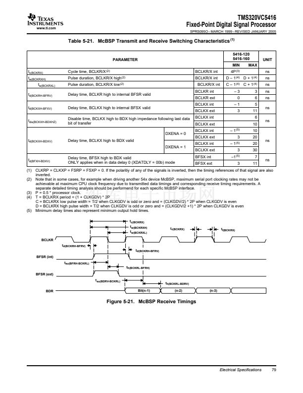
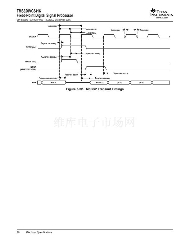
Receive clock input. BCLKR can be configured as an input or an output; it is configured as an input following
reset. BCLKR serves as the serial shift clock for the buffered serial port receiver.
Serial data receive input
Frame synchronization pulse for receive input. BFSR can be configured as an input or an output; it is configured
as an input following reset. The BFSR pulse initiates the receive data process over BDR.
Transmit clock. BCLKX serves as the serial shift clock for the McBSP transmitter. BCLKX can be configured as
an input or an output, and is configured as an input following reset. BCLKX enters the high-impedance state
when OFF goes low.
Serial data transmit output. BDX is placed in the high-impedance state when not transmitting, when RS is
asserted, or when OFF is low.
Frame synchronization pulse for transmit input/output. The BFSX pulse initiates the data transmit process over
BDX. BFSX can be configured as an input or an output, and is configured as an input following reset. BFSX
goes into the high-impedance state when OFF is low.
I/O/Z
O/Z
I/O/Z
14
Introduction


 1
1
 2
2
 3
3
 4
4
 5
5
 6
6
 7
7
 8
8
 9
9
 10
10
 11
11
 12
12
 13
13
 14
14
 15
15
 16
16
 17
17
 18
18
 19
19
 20
20
 21
21
 22
22
 23
23
 24
24
 25
25
 26
26
 27
27
 28
28
 29
29
 30
30
 31
31
 32
32
 33
33
 34
34
 35
35
 36
36
 37
37
 38
38
 39
39
 40
40
 41
41
 42
42
 43
43
 44
44
 45
45
 46
46
 47
47
 48
48
 49
49
 50
50
 51
51
 52
52
 53
53
 54
54
 55
55
 56
56
 57
57
 58
58
 59
59
 60
60
 61
61
 62
62
 63
63
 64
64
 65
65
 66
66
 67
67
 68
68
 69
69
 70
70
 71
71
 72
72
 73
73
 74
74
 75
75
 76
76
 77
77
 78
78
 79
79
 80
80
 81
81
 82
82
 83
83
 84
84
 85
85
 86
86
 87
87
 88
88
 89
89
 90
90
 91
91
 92
92
 93
93
 94
94
 95
95
 96
96
 97
97
 98
98
