www.ti.com
TMS320VC5416
Fixed-Point Digital Signal Processor
SPRS095O 鈥?MARCH 1999 鈥?REVISED JANUARY 2005
Contents
Revision History
...........................................................................................................................
2
1
TMS320VC5416 Features
.......................................................................................................
9
2
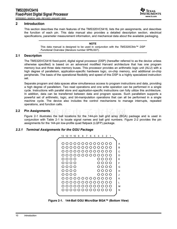
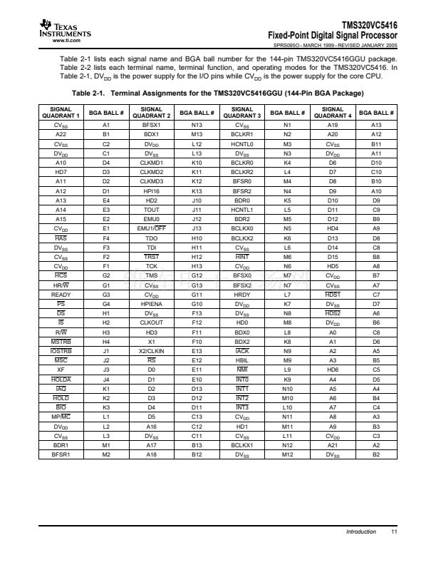
Introduction
.......................................................................................................................
10
2.1
2.2
Description
..................................................................................................................
Pin Assignments
............................................................................................................
2.2.1
Terminal Assignments for the GGU Package
...............................................................
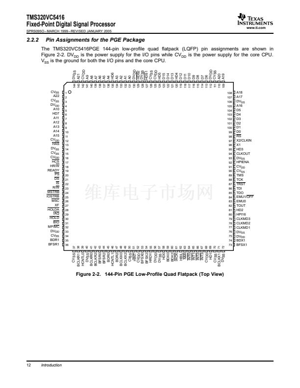
2.2.2
Pin Assignments for the PGE Package
......................................................................
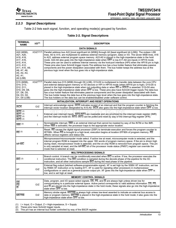
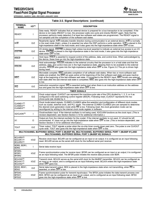
2.2.3
Signal Descriptions
..............................................................................................
Memory
......................................................................................................................
3.1.1
Data Memory
.....................................................................................................
3.1.2
Program Memory
................................................................................................
3.1.3
Extended Program Memory
...................................................................................
On-Chip ROM With Bootloader
...........................................................................................
On-Chip RAM
...............................................................................................................
On-Chip Memory Security
.................................................................................................
Memory Map
................................................................................................................
3.5.1
Relocatable Interrupt Vector Table
............................................................................
On-Chip Peripherals
.......................................................................................................
3.6.1
Software-Programmable Wait-State Generator
.............................................................
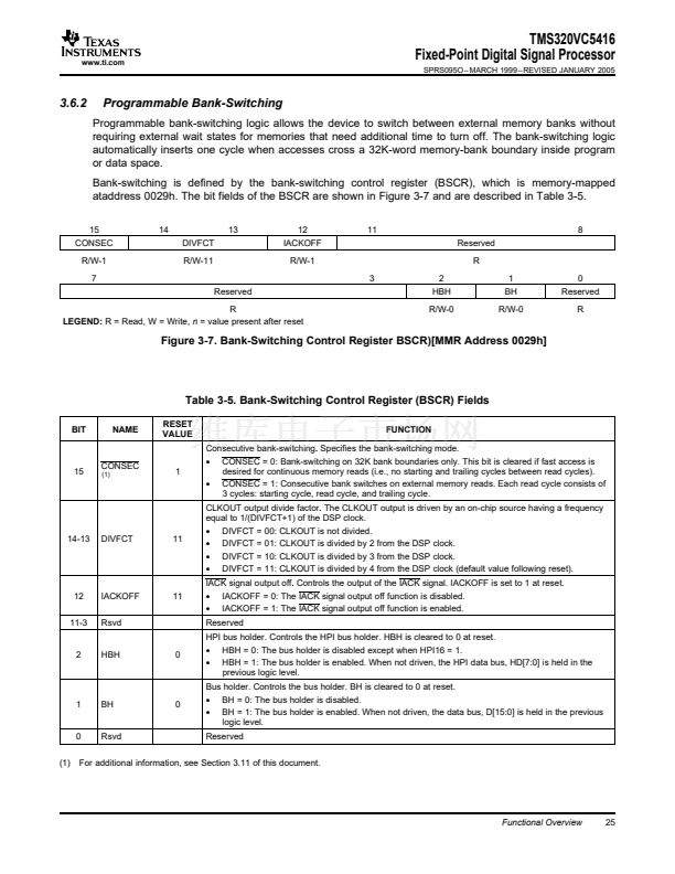
3.6.2
Programmable Bank-Switching
................................................................................
3.6.3
Bus Holders
......................................................................................................
Parallel I/O Ports
...........................................................................................................
3.7.1
Enhanced 8-/16-Bit Host-Port Interface (HPI8/16)
..........................................................
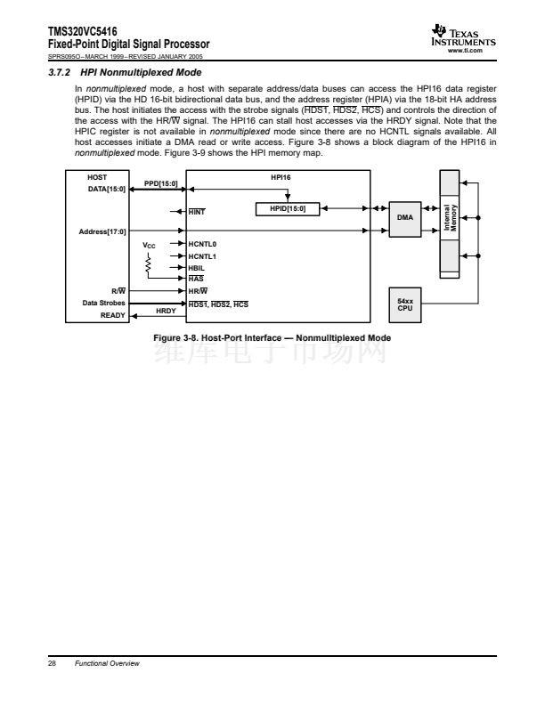
3.7.2
HPI Nonmultiplexed Mode
......................................................................................
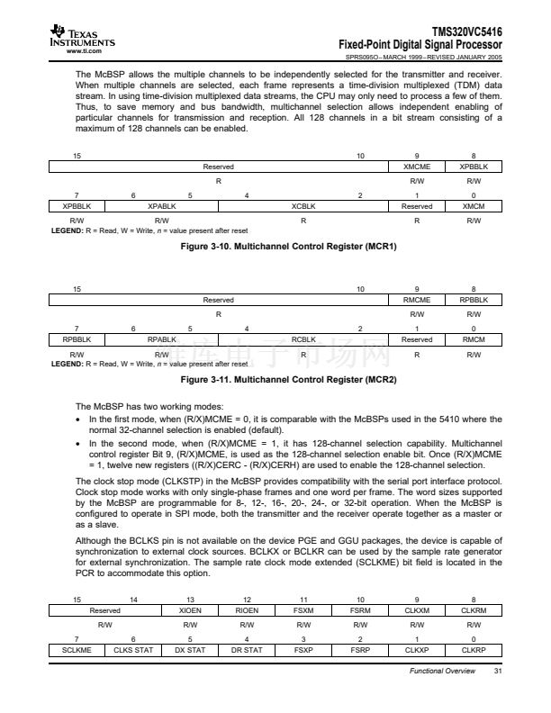
Multichannel Buffered Serial Ports (McBSPs)
..........................................................................
Hardware Timer
............................................................................................................
Clock Generator
............................................................................................................
Enhanced External Parallel Interface (XIO2)
...........................................................................
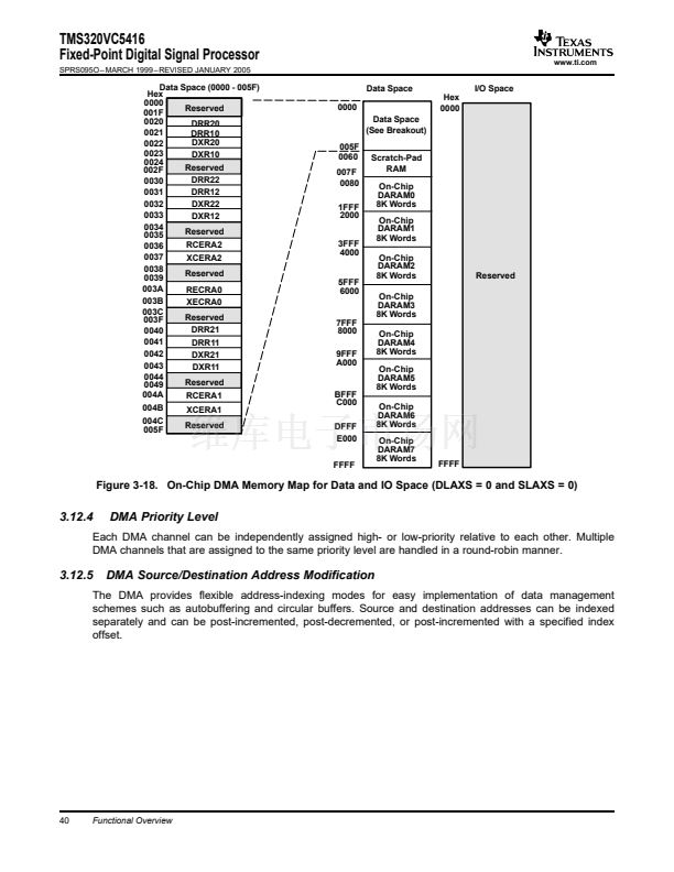
DMA Controller
.............................................................................................................
3.12.1 Features
..........................................................................................................
3.12.2 DMA External Access
...........................................................................................
3.12.3 DMA Memory Maps
.............................................................................................
3.12.4 DMA Priority Level
...............................................................................................
3.12.5 DMA Source/Destination Address Modification
.............................................................
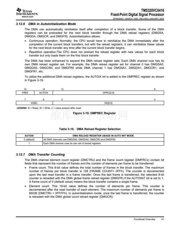
3.12.6 DMA in Autoinitialization Mode
................................................................................
3.12.7 DMA Transfer Counting
.........................................................................................
3.12.8 DMA Transfer in Doubleword Mode
..........................................................................
3.12.9 DMA Channel Index Registers
.................................................................................
3.12.10 DMA Interrupts
..................................................................................................
3.12.11 DMA Controller Synchronization Events
....................................................................
General-Purpose I/O Pins
.................................................................................................
3.13.1 McBSP Pins as General-Purpose I/O
.........................................................................
3.13.2 HPI Data Pins as General-Purpose I/O
......................................................................
Device ID Register
.........................................................................................................
Memory-Mapped Registers
...............................................................................................
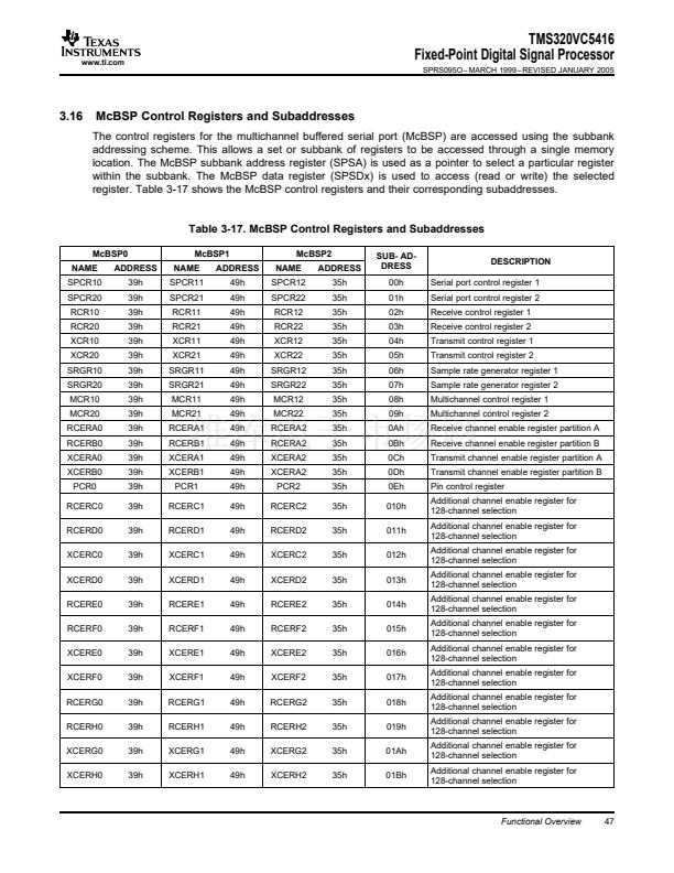
McBSP Control Registers and Subaddresses
..........................................................................
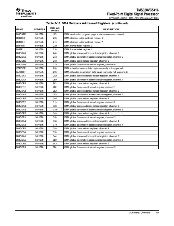
DMA Subbank Addressed Registers
....................................................................................
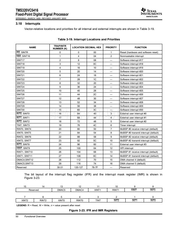
Interrupts
....................................................................................................................
Contents
10
10
10
12
13
16
16
18
18
18
19
19
20
21
23
23
25
26
26
27
28
30
32
32
34
37
37
37
39
40
40
41
41
42
42
42
42
43
43
44
44
45
47
48
50
3
3
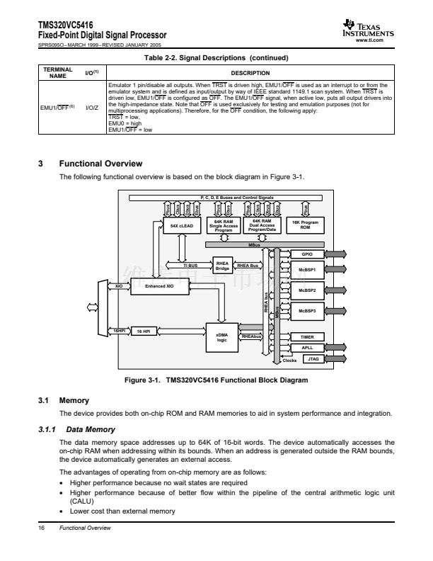
Functional Overview
...........................................................................................................
16
3.1
3.2
3.3
3.4
3.5
3.6
3.7
3.8
3.9
3.10
3.11
3.12
3.13
3.14
3.15
3.16
3.17
3.18


 1
1
 2
2
 3
3
 4
4
 5
5
 6
6
 7
7
 8
8
 9
9
 10
10
 11
11
 12
12
 13
13
 14
14
 15
15
 16
16
 17
17
 18
18
 19
19
 20
20
 21
21
 22
22
 23
23
 24
24
 25
25
 26
26
 27
27
 28
28
 29
29
 30
30
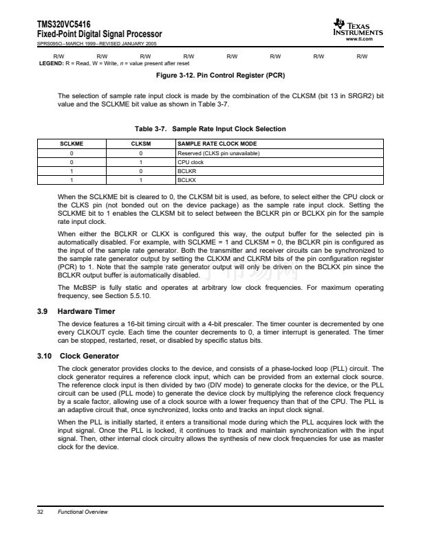
 31
31
 32
32
 33
33
 34
34
 35
35
 36
36
 37
37
 38
38
 39
39
 40
40
 41
41
 42
42
 43
43
 44
44
 45
45
 46
46
 47
47
 48
48
 49
49
 50
50
 51
51
 52
52
 53
53
 54
54
 55
55
 56
56
 57
57
 58
58
 59
59
 60
60
 61
61
 62
62
 63
63
 64
64
 65
65
 66
66
 67
67
 68
68
 69
69
 70
70
 71
71
 72
72
 73
73
 74
74
 75
75
 76
76
 77
77
 78
78
 79
79
 80
80
 81
81
 82
82
 83
83
 84
84
 85
85
 86
86
 87
87
 88
88
 89
89
 90
90
 91
91
 92
92
 93
93
 94
94
 95
95
 96
96
 97
97
 98
98
