www.ti.com
TMS320VC5416
Fixed-Point Digital Signal Processor
SPRS095O 鈥?MARCH 1999 鈥?REVISED JANUARY 2005
List of Figures
2-1
2-2
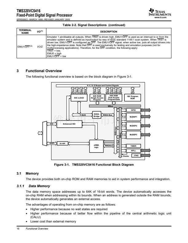
3-1
3-2
3-3
3-4
3-5
3-6
3-7
3-8
3-9
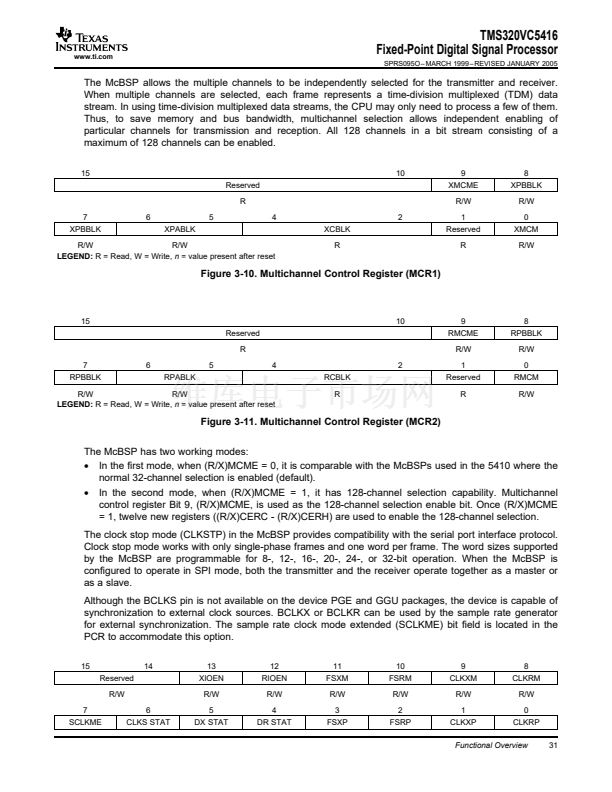
3-10
3-11
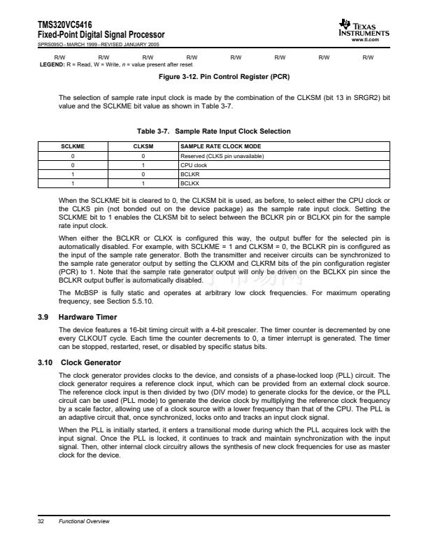
3-12
3-13
3-14
3-15
3-16
3-17
3-18
3-19
3-20
3-21
3-22
3-23
5-1
5-2
5-3
5-4
5-5
5-6
5-7
5-8
5-9
5-10
5-11
5-12
5-13
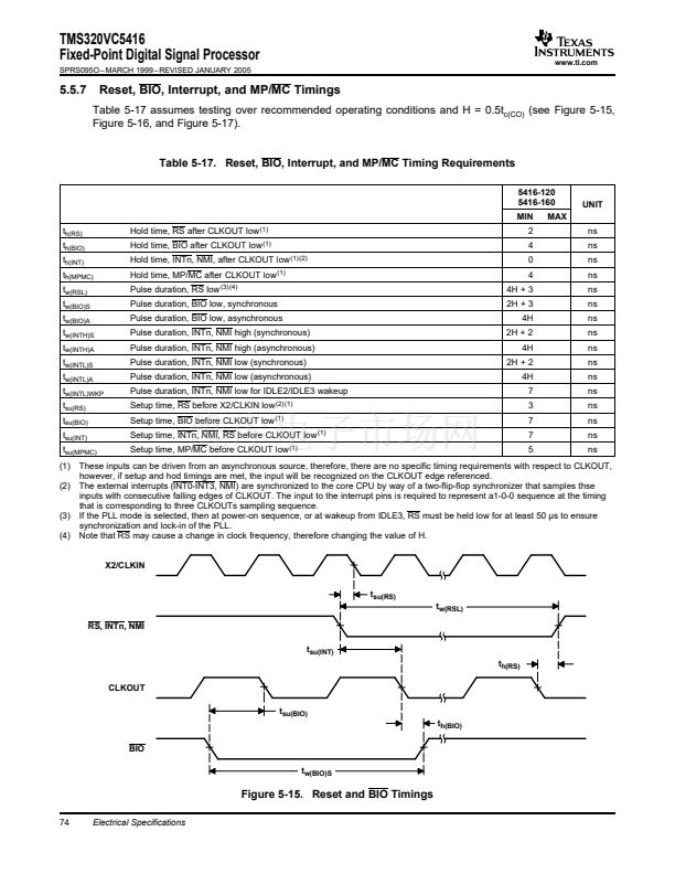
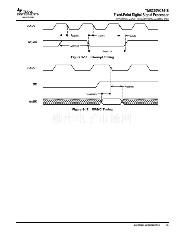
5-14
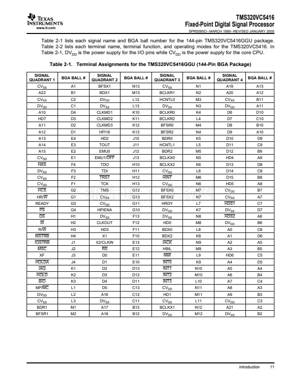
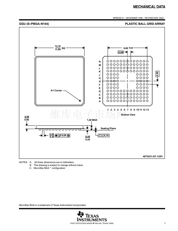
144-Ball GGU MicroStar BGA鈩?(Bottom View)
.............................................................................
10
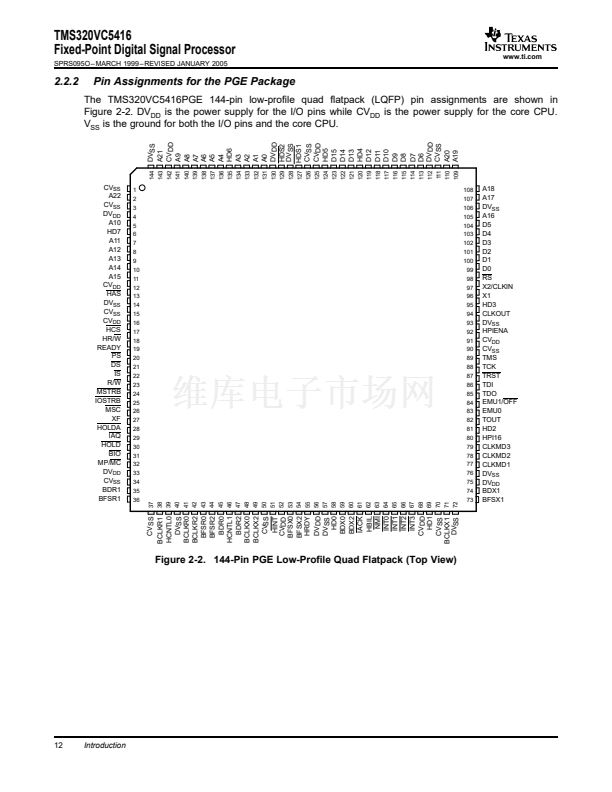
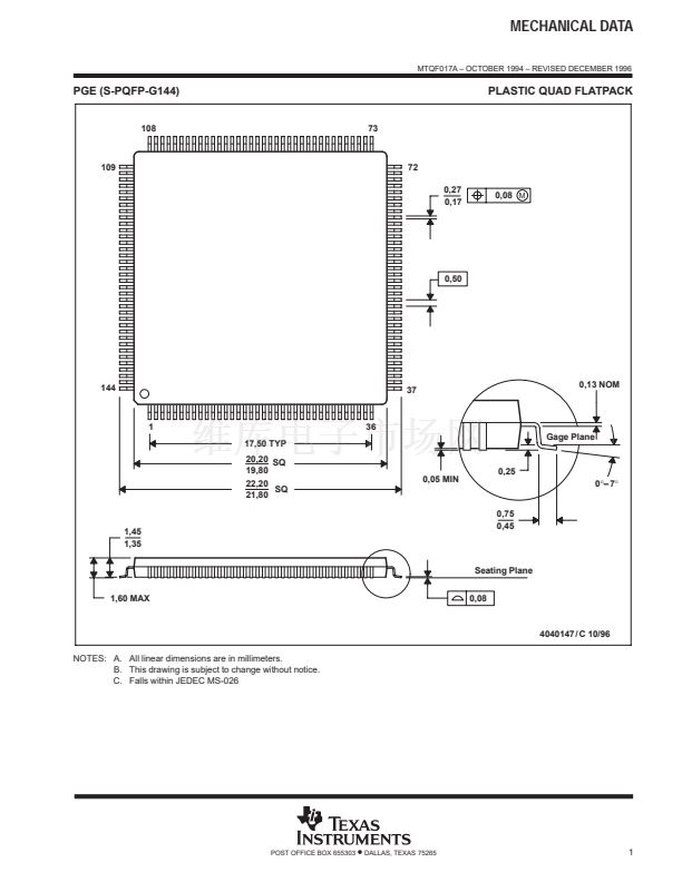
144-Pin PGE Low-Profile Quad Flatpack (Top View)
.......................................................................
12
TMS320VC5416 Functional Block Diagram
..................................................................................
16
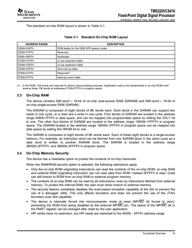
Program and Data Memory Map
................................................................................................
20
...............................................................................................
Process Mode Status Register
..................................................................................................
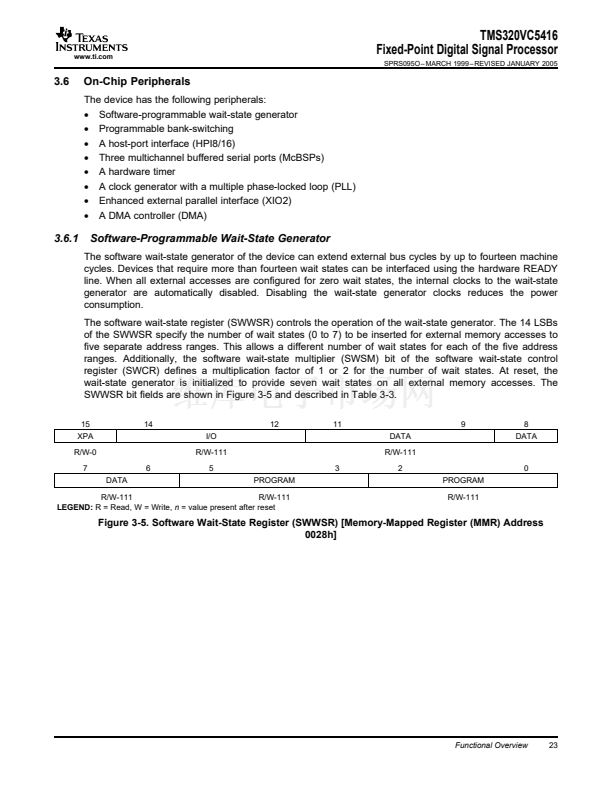
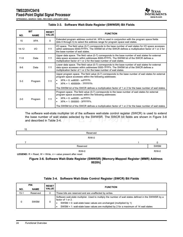
Software Wait-State Register (SWWSR) [Memory-Mapped Register (MMR) Address 0028h]
.........................
Software Wait-State Register (SWWSR) [Memory-Mapped Register (MMR) Address 0028h]
.........................
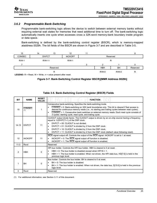
Bank-Switching Control Register BSCR)[MMR Address 0029h]
...........................................................
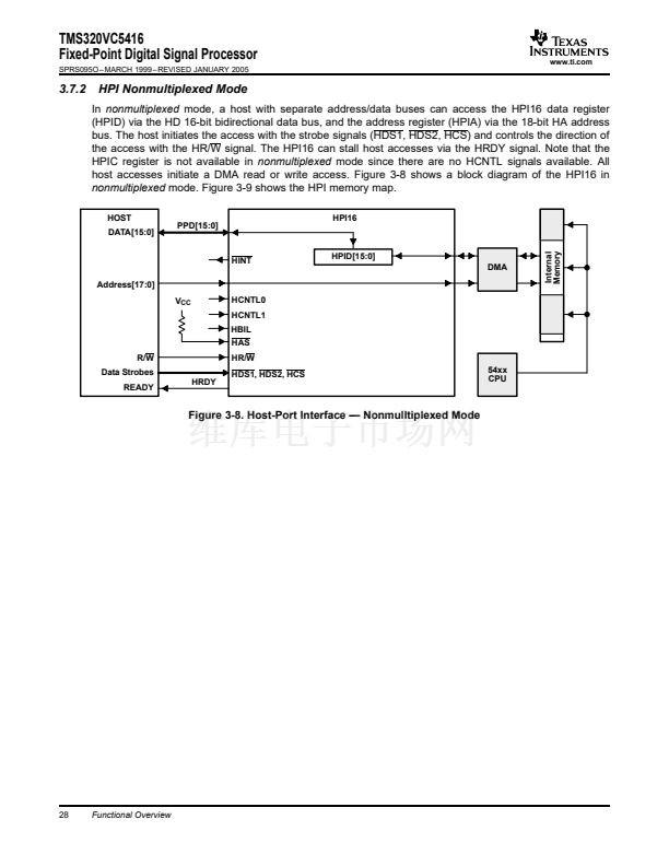
Host-Port Interface 鈥?Nonmulltiplexed Mode
.................................................................................
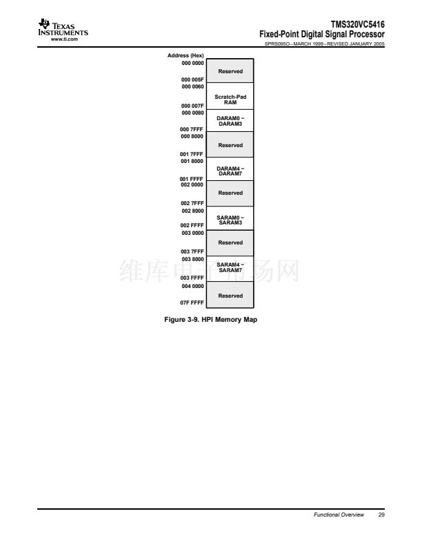
HPI Memory Map
.................................................................................................................
Multichannel Control Register (MCR1)
.........................................................................................
Multichannel Control Register (MCR2)
.........................................................................................
Pin Control Register (PCR)
......................................................................................................
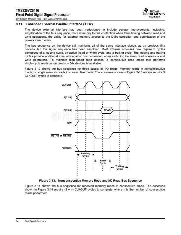
Nonconsecutive Memory Read and I/O Read Bus Sequence
.............................................................
Consecutive Memory Read Bus Sequence (n = 3 reads)
..................................................................
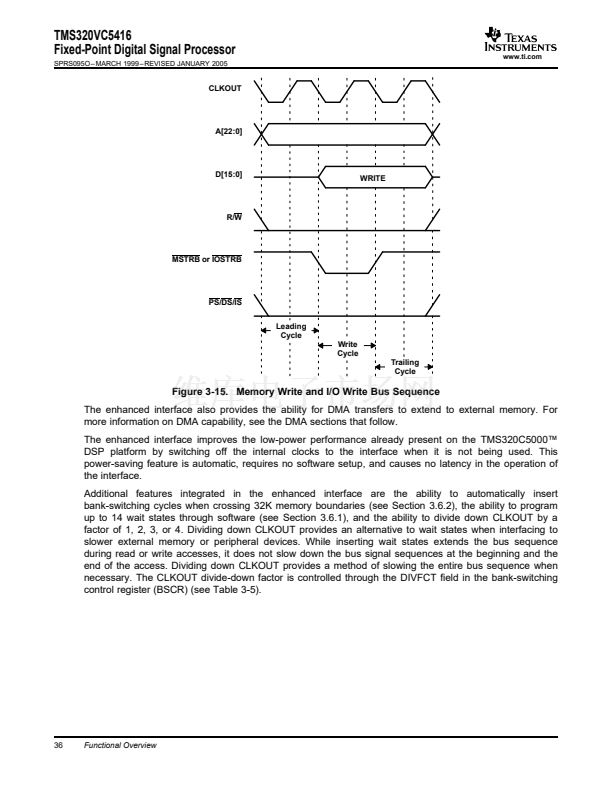
Memory Write and I/O Write Bus Sequence
.................................................................................
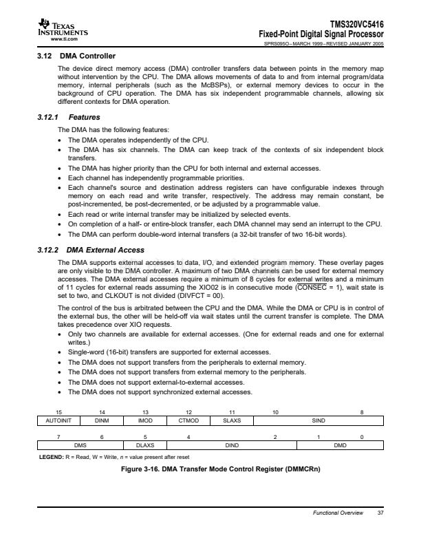
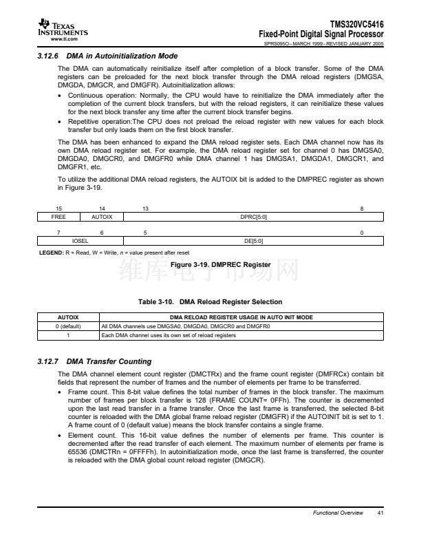
DMA Transfer Mode Control Register (DMMCRn)
...........................................................................
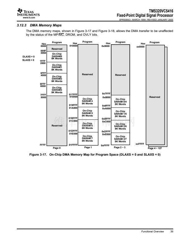
On-Chip DMA Memory Map for Program Space (DLAXS = 0 and SLAXS = 0)
.........................................
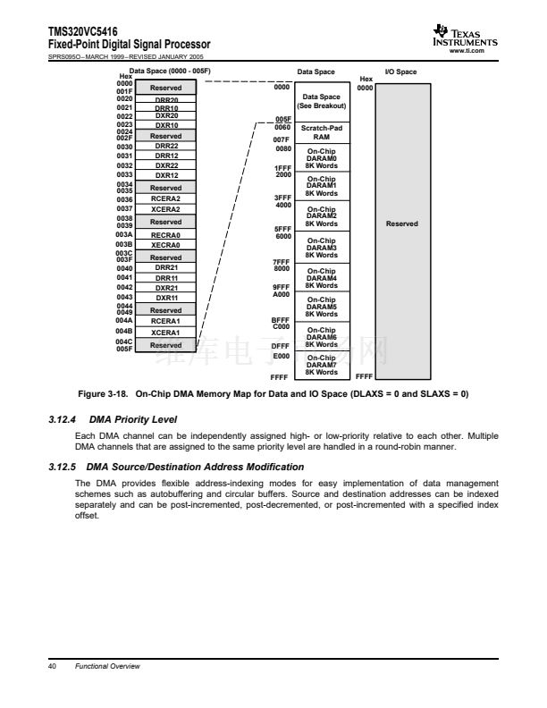
On-Chip DMA Memory Map for Data and IO Space (DLAXS = 0 and SLAXS = 0)
....................................
DMPREC Register
................................................................................................................
General-Purpose I/O Control Register (GPIOCR) [MMR Address 003Ch]
................................................
General-Purpose I/O Status Register (GPIOSR) [MMR Address 003Dh]
.................................................
Device ID Register (CSIDR) [MMR Address 003Eh]
.........................................................................
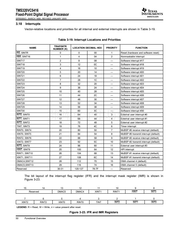
IFR and IMR Registers
...........................................................................................................
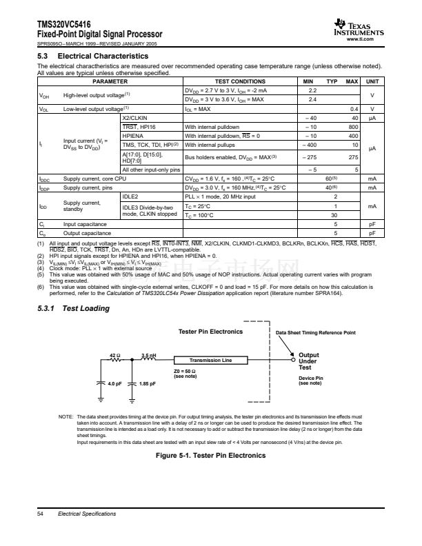
Tester Pin Electronics
............................................................................................................
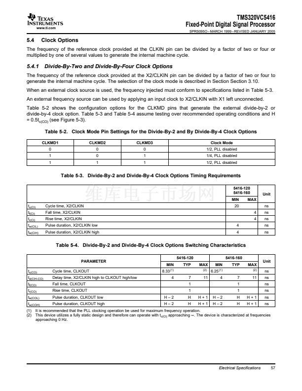
Internal Divide-By-Two Clock Option With External Crystal
...............................................................
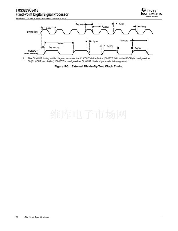
External Divide-By-Two Clock Timing
.........................................................................................
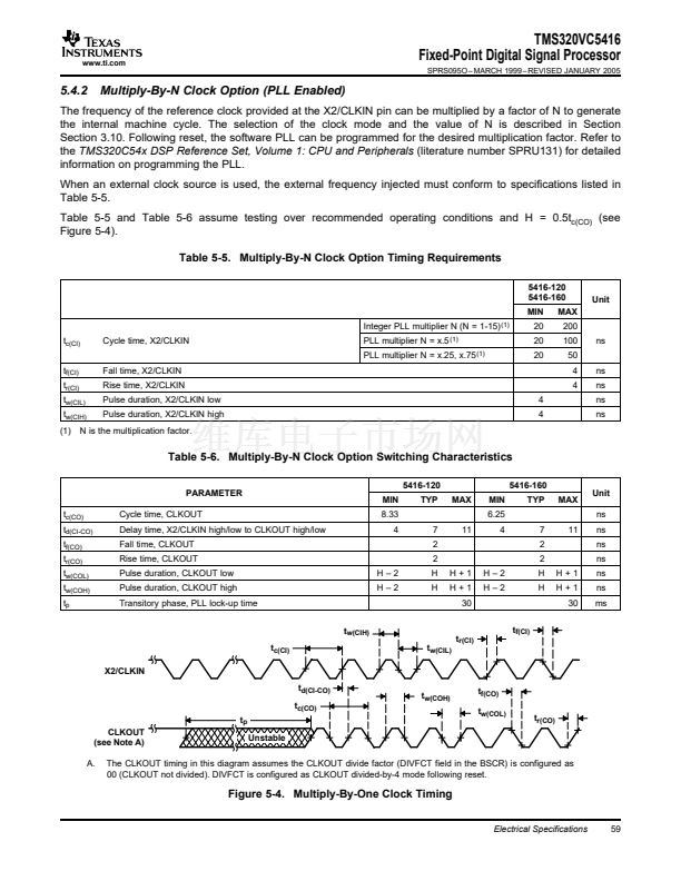
Multiply-By-One Clock Timing
..................................................................................................
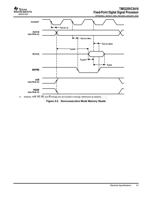
Nonconsecutive Mode Memory Reads
.......................................................................................
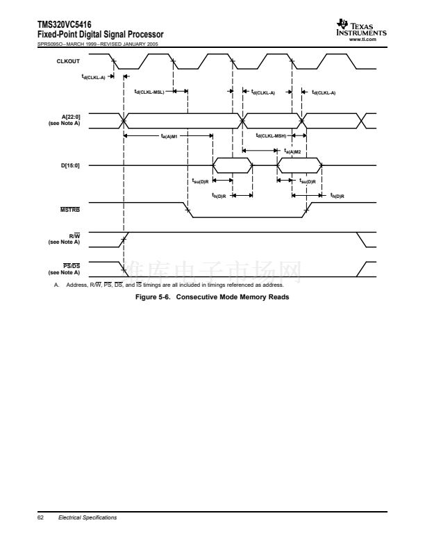
Consecutive Mode Memory Reads
............................................................................................
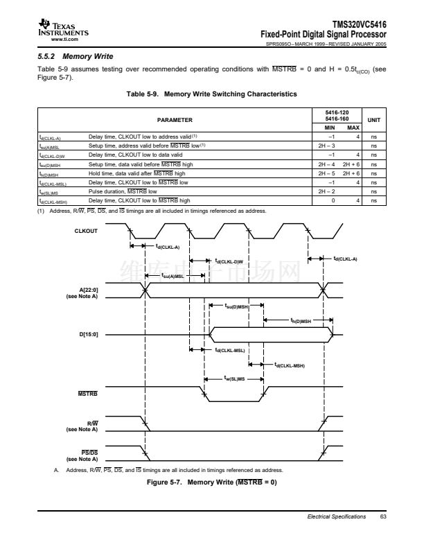
Memory Write (MSTRB = 0)
....................................................................................................
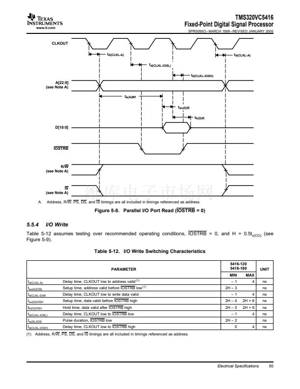
Parallel I/O Port Read (IOSTRB = 0)
.........................................................................................
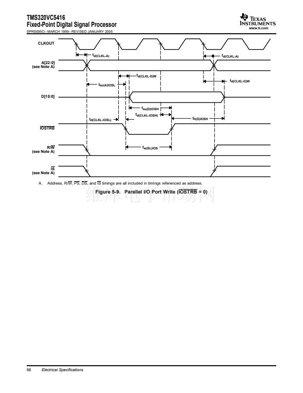
Parallel I/O Port Write (IOSTRB = 0)
..........................................................................................
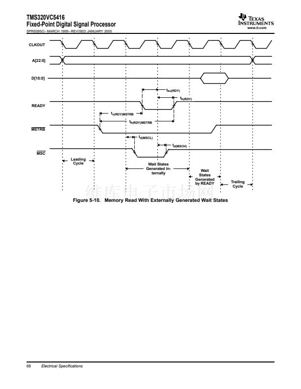
Memory Read With Externally Generated Wait States
.....................................................................
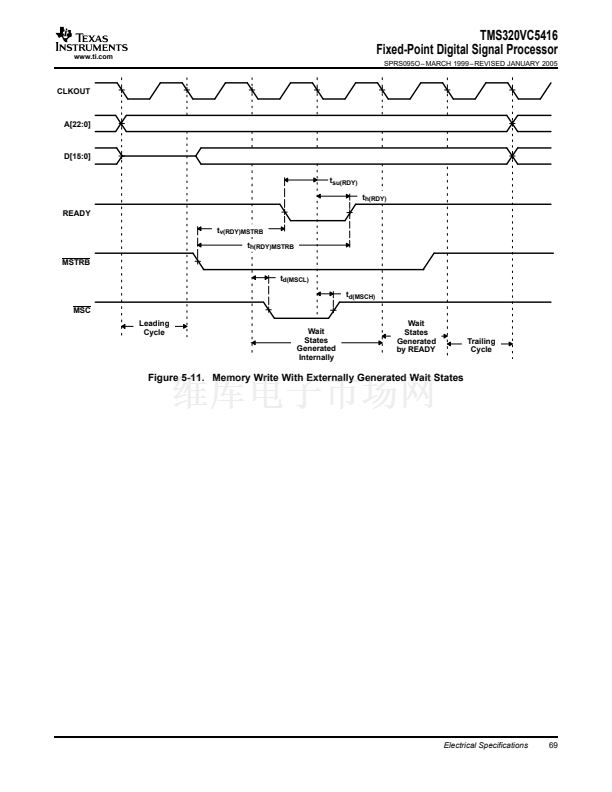
Memory Write With Externally Generated Wait States
.....................................................................
I/O Read With Externally Generated Wait States
...........................................................................
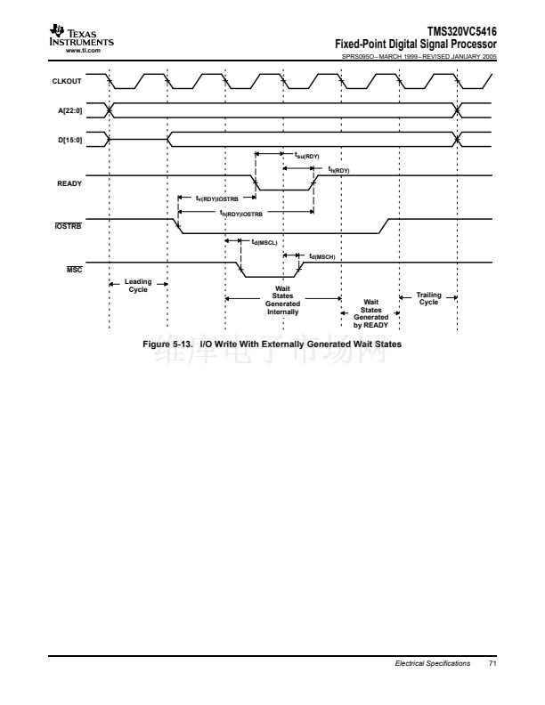
I/O Write With Externally Generated Wait States
...........................................................................
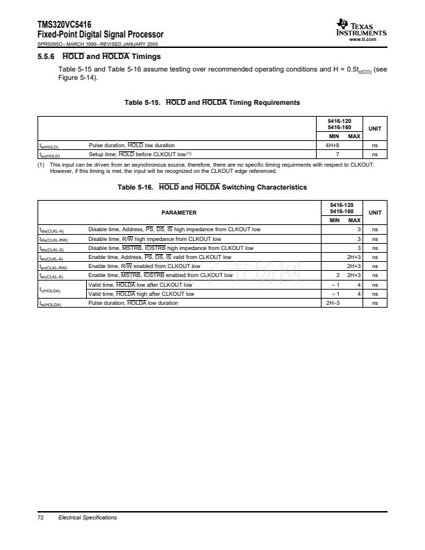
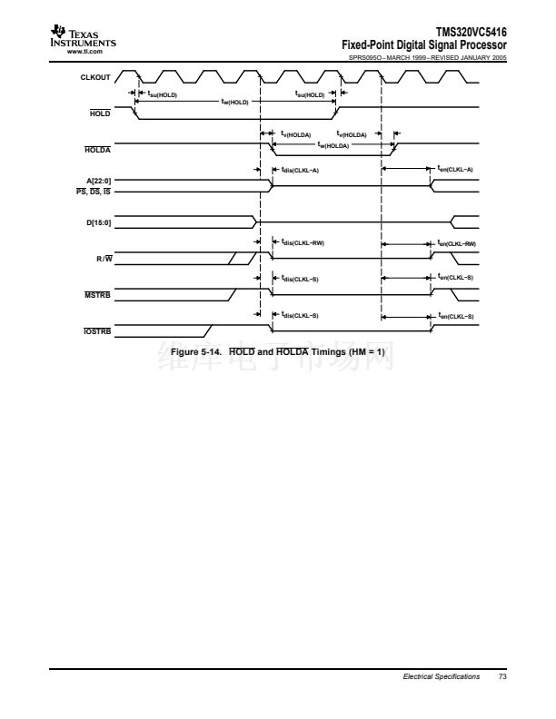
HOLD and HOLDA Timings (HM = 1)
.........................................................................................
Extended Program Memory Map
List of Figures
21
22
23
24
25
28
29
31
31
32
34
35
36
37
39
40
41
44
44
44
50
54
56
58
59
61
62
63
65
66
68
69
70
71
73
5


 1
1
 2
2
 3
3
 4
4
 5
5
 6
6
 7
7
 8
8
 9
9
 10
10
 11
11
 12
12
 13
13
 14
14
 15
15
 16
16
 17
17
 18
18
 19
19
 20
20
 21
21
 22
22
 23
23
 24
24
 25
25
 26
26
 27
27
 28
28
 29
29
 30
30
 31
31
 32
32
 33
33
 34
34
 35
35
 36
36
 37
37
 38
38
 39
39
 40
40
 41
41
 42
42
 43
43
 44
44
 45
45
 46
46
 47
47
 48
48
 49
49
 50
50
 51
51
 52
52
 53
53
 54
54
 55
55
 56
56
 57
57
 58
58
 59
59
 60
60
 61
61
 62
62
 63
63
 64
64
 65
65
 66
66
 67
67
 68
68
 69
69
 70
70
 71
71
 72
72
 73
73
 74
74
 75
75
 76
76
 77
77
 78
78
 79
79
 80
80
 81
81
 82
82
 83
83
 84
84
 85
85
 86
86
 87
87
 88
88
 89
89
 90
90
 91
91
 92
92
 93
93
 94
94
 95
95
 96
96
 97
97
 98
98
