www.ti.com
TMS320VC5416
Fixed-Point Digital Signal Processor
SPRS095O 鈥?MARCH 1999 鈥?REVISED JANUARY 2005
List of Tables
2-1
2-2
3-1
3-2
3-3
3-4
3-5
3-6
3-7
3-8
3-9
3-10
3-11
3-12
3-13
3-14
3-15
3-16
3-17
3-18
3-19
5-1
5-2
5-3
5-4
5-5
5-6
5-7
5-8
5-9
5-10
5-11
5-12
5-13
5-14
5-15
5-16
5-17
5-18
.........................................
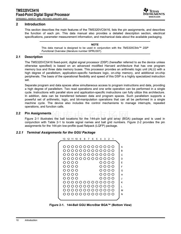
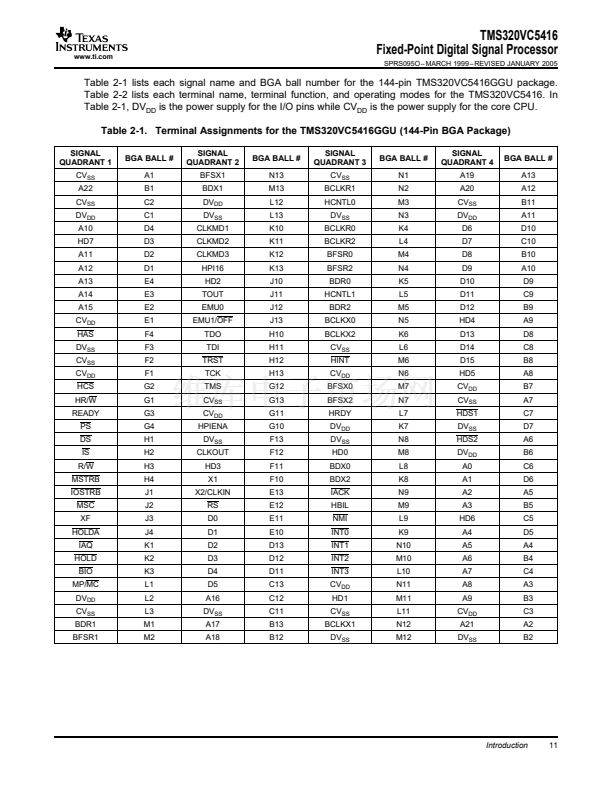
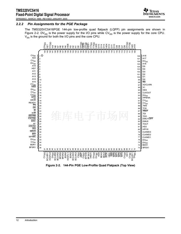
Signal Descriptions
...............................................................................................................
Standard On-Chip ROM Layout
...............................................................................................
Processor Mode Status (PMST) Register Bit Fields
........................................................................
Software Wait-State Register (SWWSR) Bit Fields
.........................................................................
Software Wait-State Control Register (SWCR) Bit Fields
..................................................................
Bank-Switching Control Register (BSCR) Fields
..............................................................................
Bus Holder Control Bits
..........................................................................................................
Sample Rate Input Clock Selection
...........................................................................................
Clock Mode Settings at Reset
.................................................................................................
DMD Section of the DMMCRn Register
......................................................................................
DMA Reload Register Selection
...............................................................................................
DMA Interrupts
...................................................................................................................
DMA Synchronization Events
..................................................................................................
DMA Channel Interrupt Selection
..............................................................................................
Device ID Register (CSIDR) Bits
................................................................................................
CPU Memory-Mapped Registers
................................................................................................
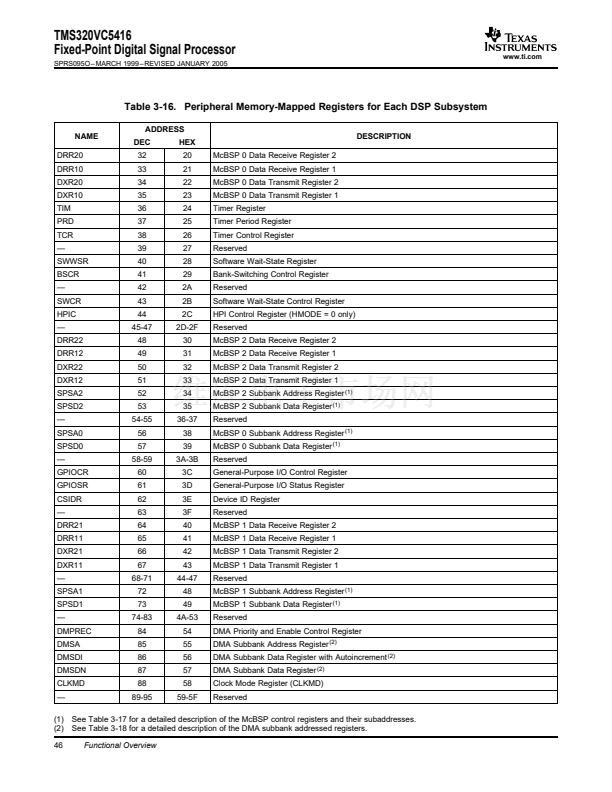
Peripheral Memory-Mapped Registers for Each DSP Subsystem
........................................................
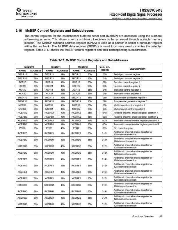
McBSP Control Registers and Subaddresses
.................................................................................
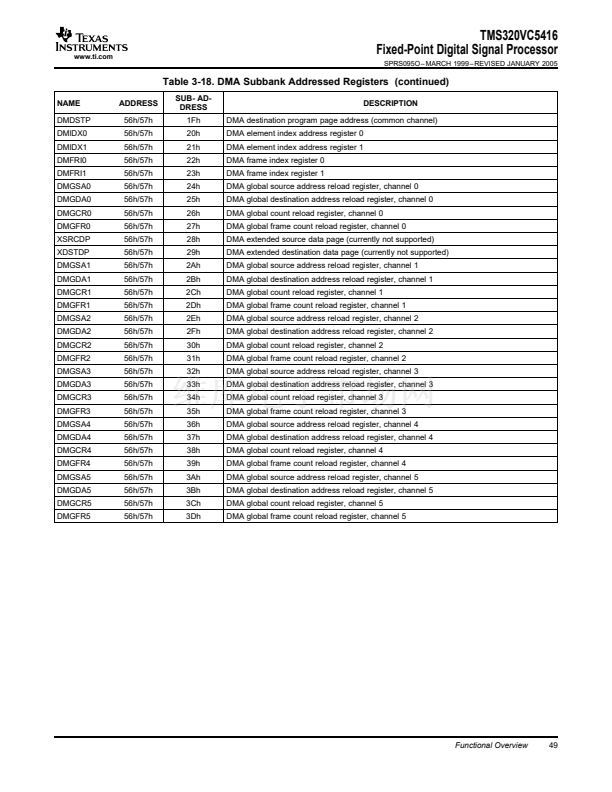
DMA Subbank Addressed Registers
...........................................................................................
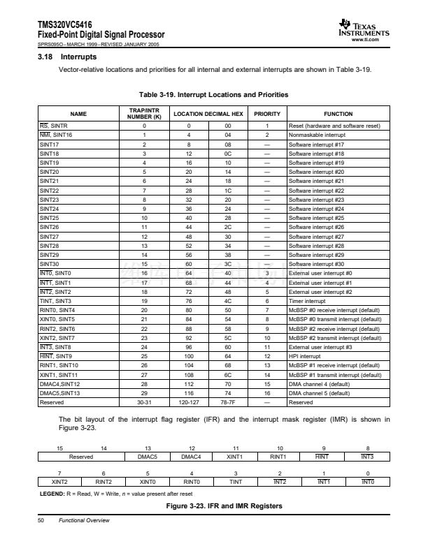
Interrupt Locations and Priorities
................................................................................................
Input Clock Frequency Characteristics
.........................................................................................
Clock Mode Pin Settings for the Divide-By-2 and By Divide-By-4 Clock Options
.......................................
Divide-By-2 and Divide-By-4 Clock Options Timing Requirements
.......................................................
Divide-By-2 and Divide-By-4 Clock Options Switching Characteristics
...................................................
Multiply-By-N Clock Option Timing Requirements
..........................................................................
Multiply-By-N Clock Option Switching Characteristics
......................................................................
Memory Read Timing Requirements
..........................................................................................
Memory Read Switching Characteristics
.....................................................................................
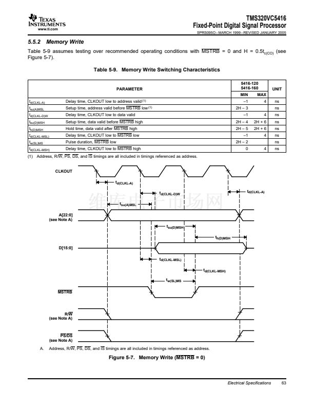
Memory Write Switching Characteristics
.....................................................................................
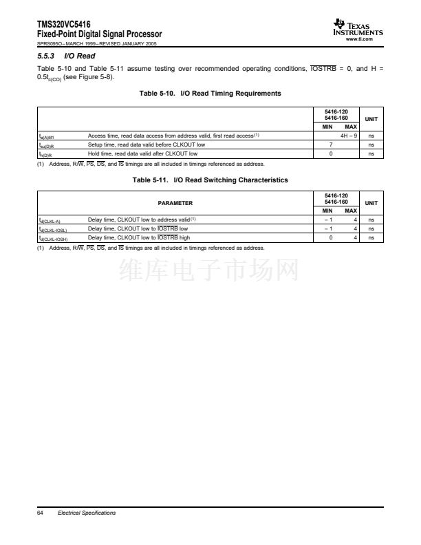
I/O Read Timing Requirements
................................................................................................
I/O Read Switching Characteristics
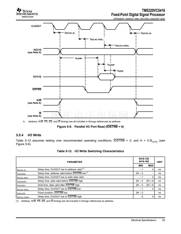
...........................................................................................
I/O Write Switching Characteristics
............................................................................................
Ready Timing Requirements for Externally Generated Wait States
......................................................
Ready Switching Characteristics for Externally Generated Wait States
..................................................
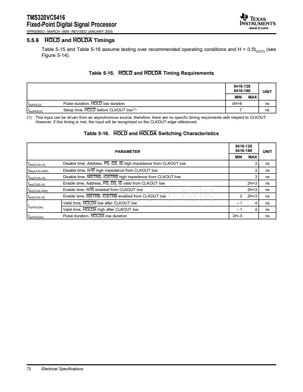
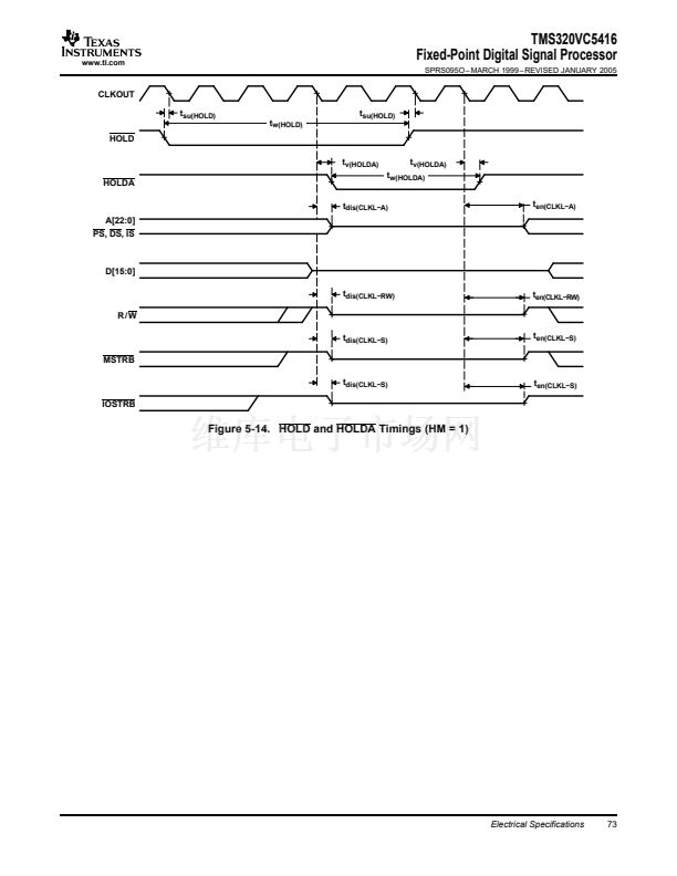
HOLD and HOLDA Timing Requirements
....................................................................................
HOLD and HOLDA Switching Characteristics
...............................................................................
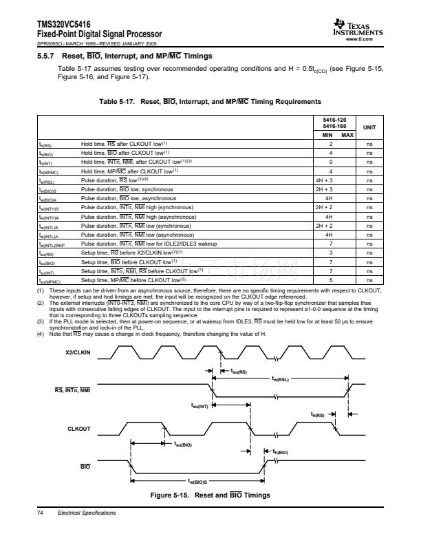
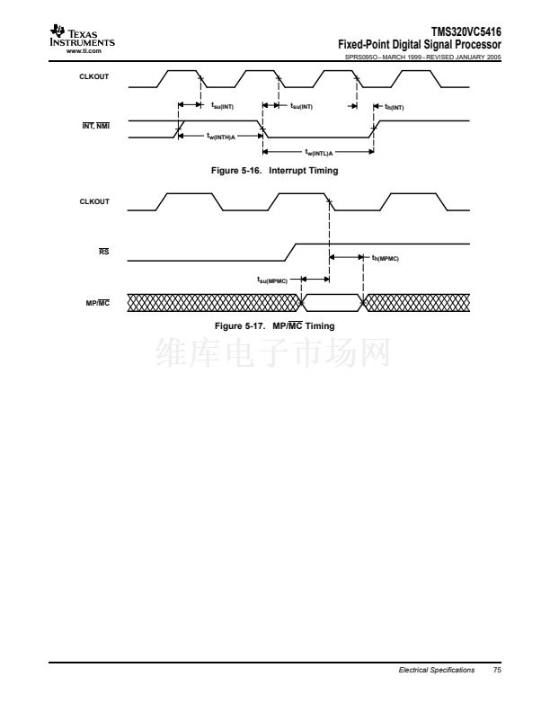
Reset, BIO, Interrupt, and MP/MC Timing Requirements
..................................................................
Instruction Acquisition (IAQ) and Interrupt Acknowledge (IACK) Switching Characteristics
...........................
Terminal Assignments for the TMS320VC5416GGU (144-Pin BGA Package)
List of Tables
11
13
19
22
24
24
25
26
32
33
38
41
42
42
43
45
45
46
47
48
50
56
57
57
57
59
59
60
60
63
64
64
65
67
67
72
72
74
76
7


 1
1
 2
2
 3
3
 4
4
 5
5
 6
6
 7
7
 8
8
 9
9
 10
10
 11
11
 12
12
 13
13
 14
14
 15
15
 16
16
 17
17
 18
18
 19
19
 20
20
 21
21
 22
22
 23
23
 24
24
 25
25
 26
26
 27
27
 28
28
 29
29
 30
30
 31
31
 32
32
 33
33
 34
34
 35
35
 36
36
 37
37
 38
38
 39
39
 40
40
 41
41
 42
42
 43
43
 44
44
 45
45
 46
46
 47
47
 48
48
 49
49
 50
50
 51
51
 52
52
 53
53
 54
54
 55
55
 56
56
 57
57
 58
58
 59
59
 60
60
 61
61
 62
62
 63
63
 64
64
 65
65
 66
66
 67
67
 68
68
 69
69
 70
70
 71
71
 72
72
 73
73
 74
74
 75
75
 76
76
 77
77
 78
78
 79
79
 80
80
 81
81
 82
82
 83
83
 84
84
 85
85
 86
86
 87
87
 88
88
 89
89
 90
90
 91
91
 92
92
 93
93
 94
94
 95
95
 96
96
 97
97
 98
98
