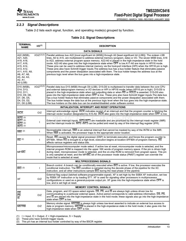
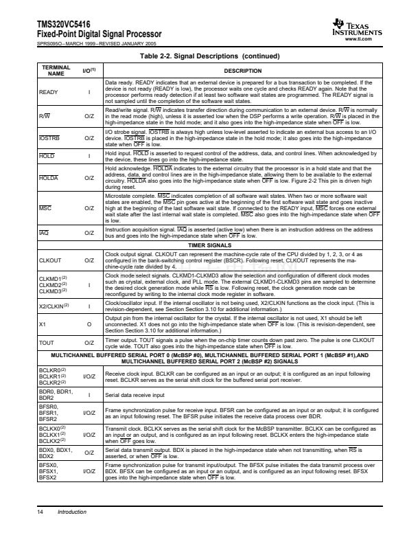
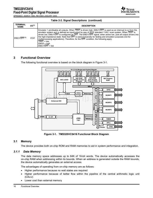
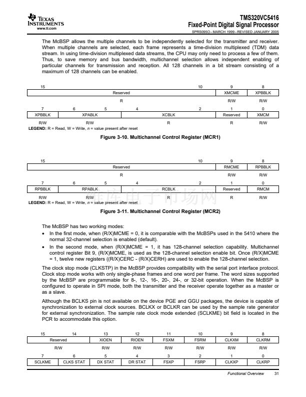
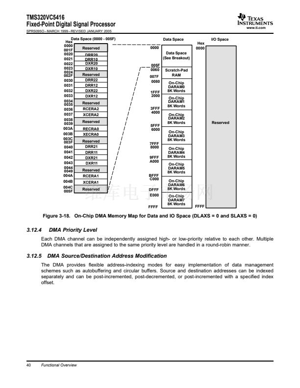
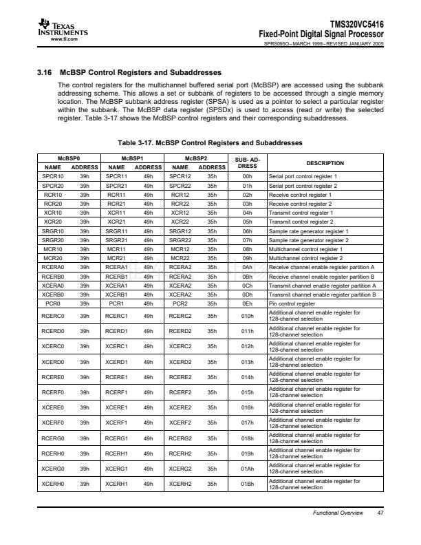
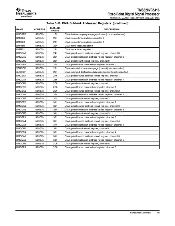
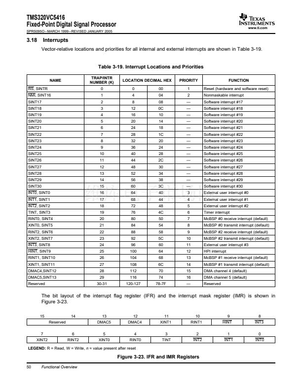
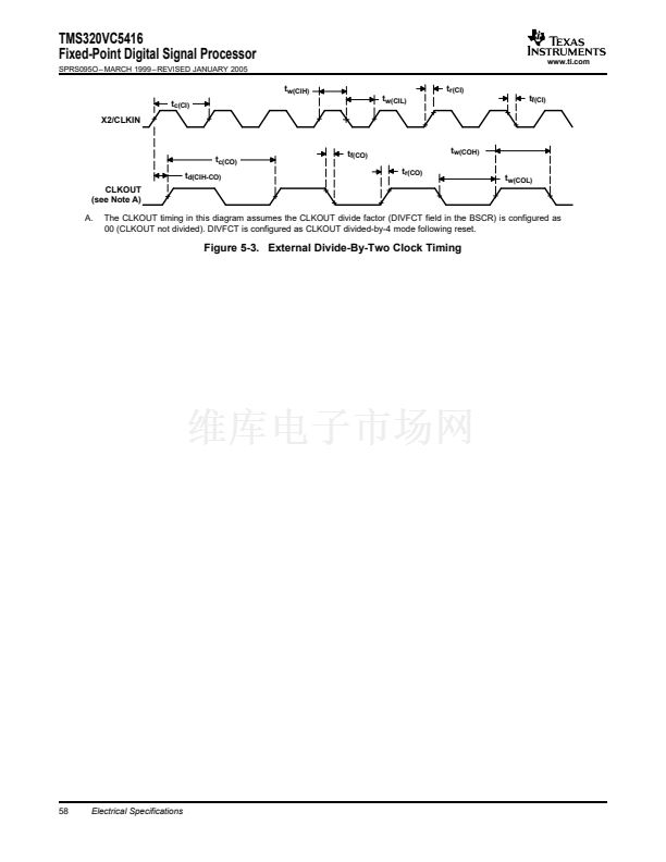
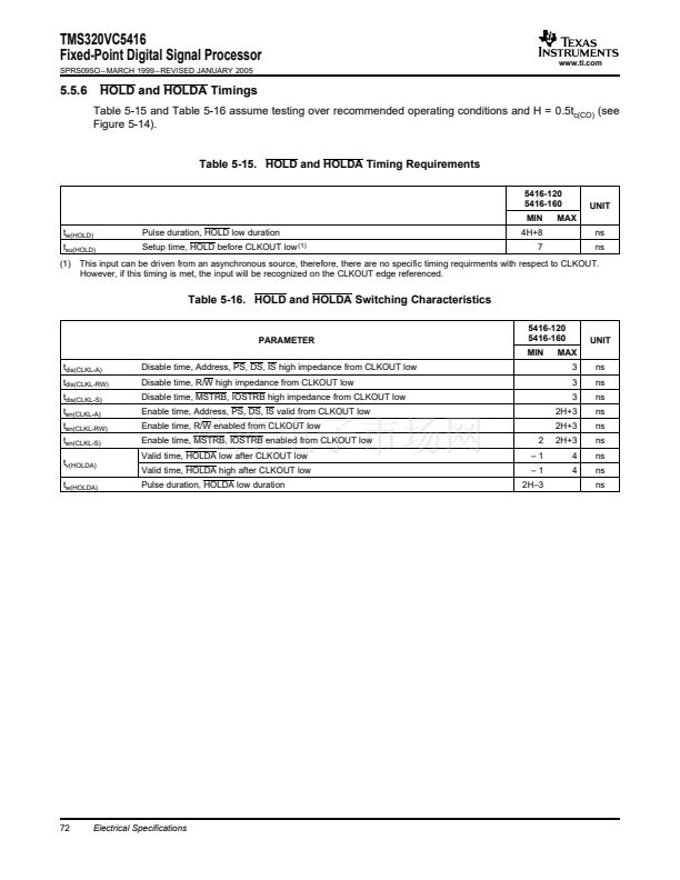
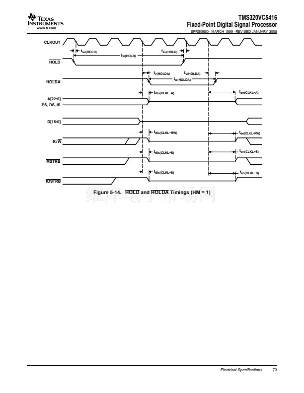
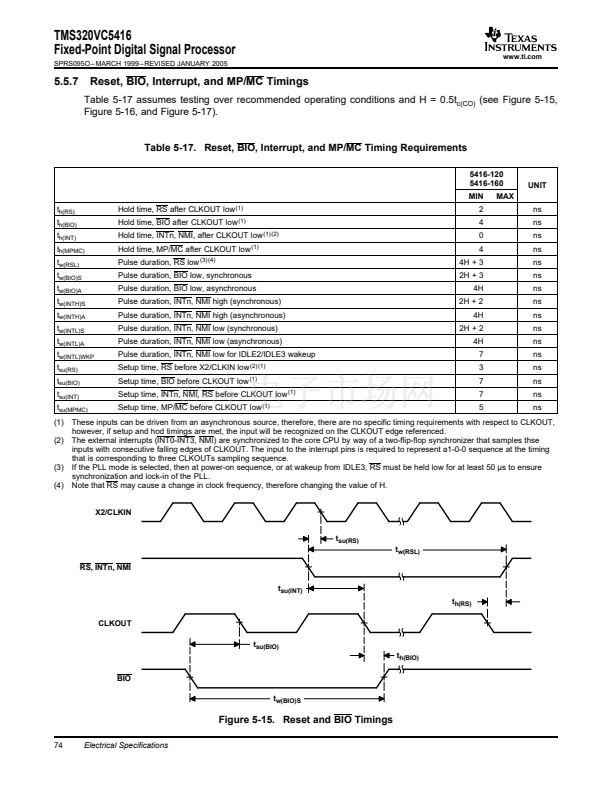
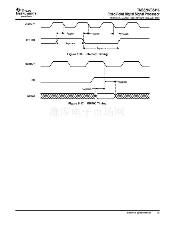
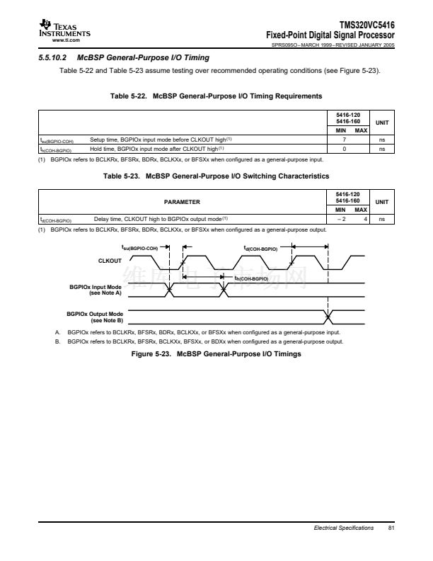
TMS320VC5416
Fixed-Point Digital Signal Processor
SPRS095O 鈥?MARCH 1999 鈥?REVISED JANUARY 2005
www.ti.com
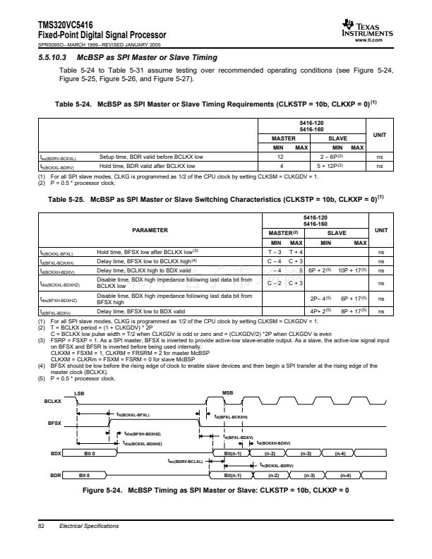
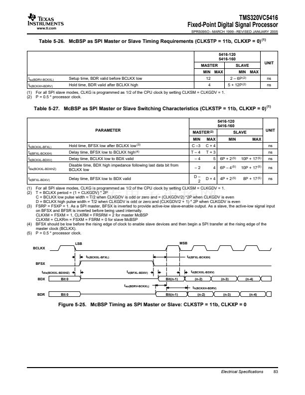
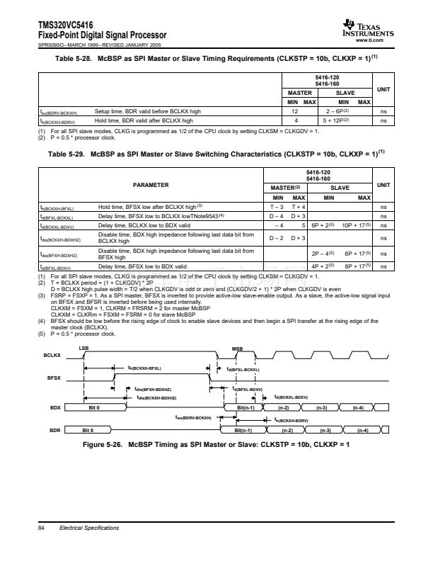
5.5.10.3
McBSP as SPI Master or Slave Timing
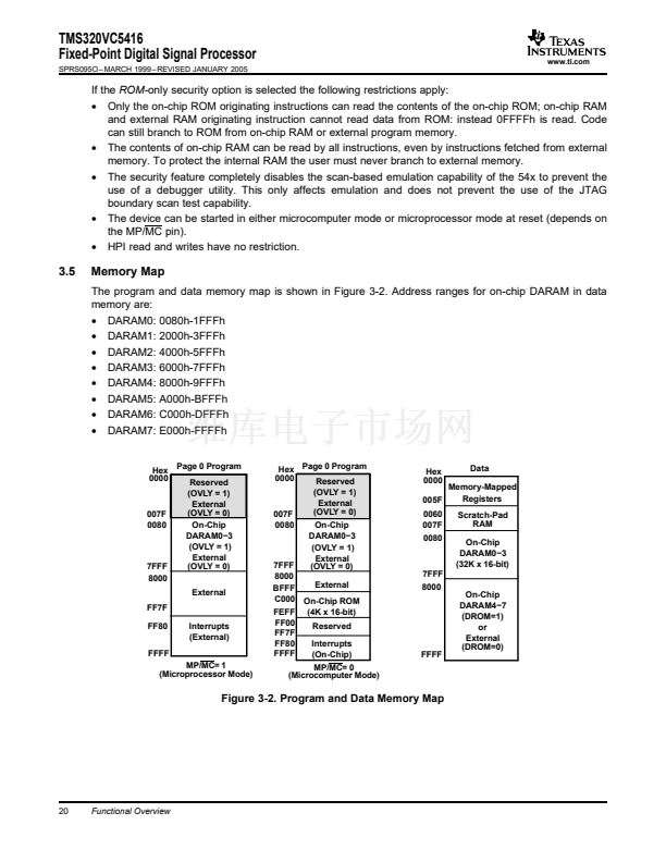
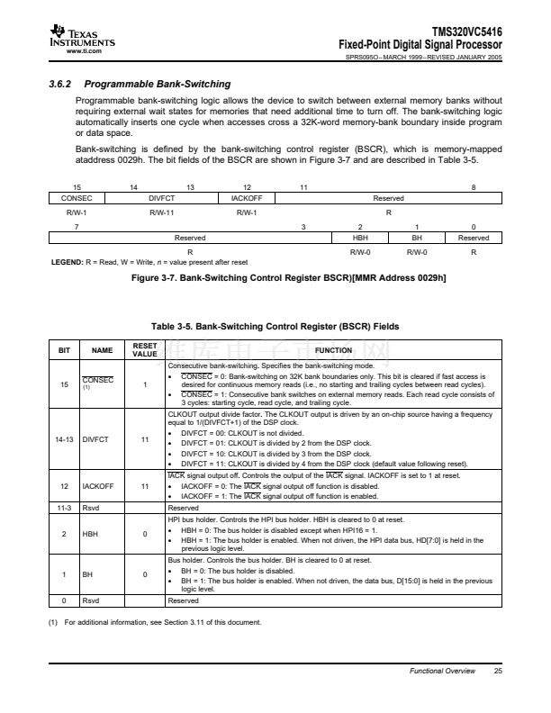
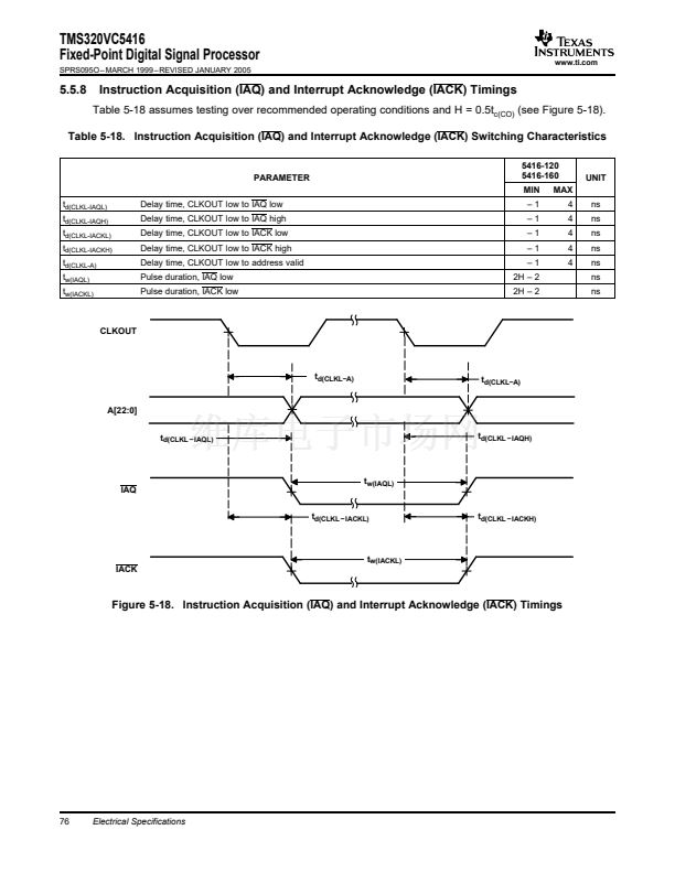
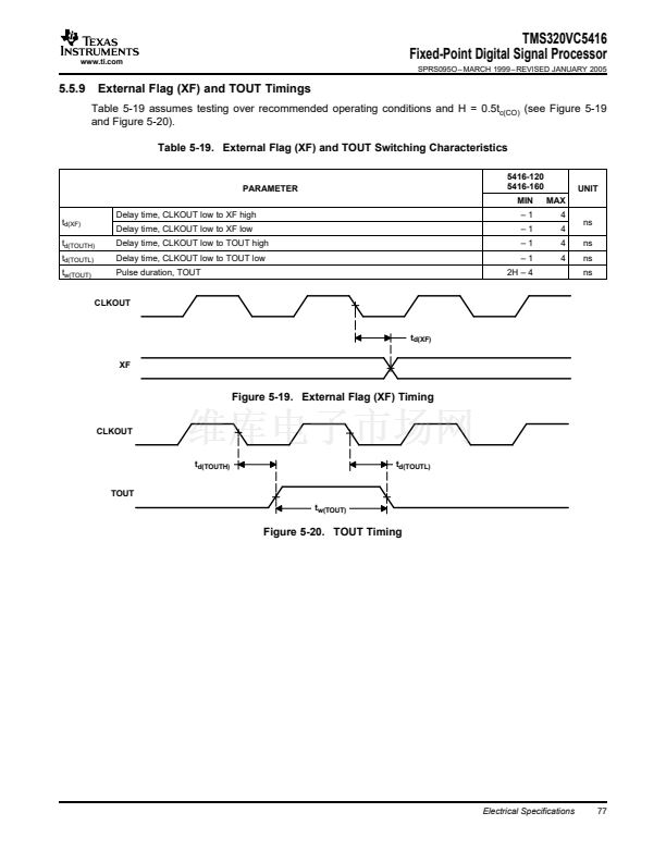
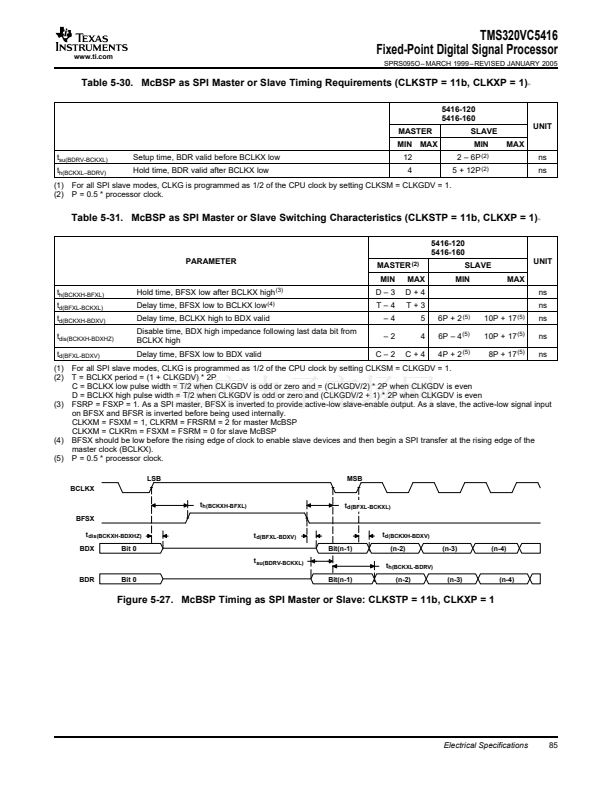
Table 5-24 to Table 5-31 assume testing over recommended operating conditions (see Figure 5-24,
Figure 5-25, Figure 5-26, and Figure 5-27).
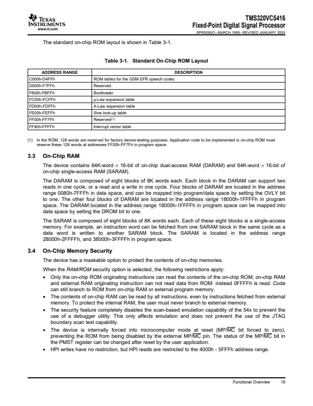
Table 5-24. McBSP as SPI Master or Slave Timing Requirements (CLKSTP = 10b, CLKXP = 0)
(1)
5416-120
5416-160
MASTER
MIN
t
su(BDRV-BCKXL)
t
h(BCKXL-BDRV)
(1)
(2)
Setup time, BDR valid before BCLKX low
Hold time, BDR valid after BCLKX low
12
4
MAX
5+
SLAVE
MIN
2 鈥?6P
(2)
12P
(2)
MAX
ns
ns
UNIT
For all SPI slave modes, CLKG is programmed as 1/2 of the CPU clock by setting CLKSM = CLKGDV = 1.
P = 0.5 * processor clock.
Table 5-25. McBSP as SPI Master or Slave Switching Characteristics (CLKSTP = 10b, CLKXP = 0)
(1)
5416-120
5416-160
PARAMETER
MASTER
(2)
MIN
t
h(BCKXL-BFXL)
t
d(BFXL-BCKXH)
t
d(BCKXH-BDXV)
t
dis(BCKXL-BDXHZ)
t
dis(BFXH-BDXHZ)
t
d(BFXL-BDXV)
(1)
(2)
(3)
Hold time, BFSX low after BCLKX low
(3)
Delay time, BFSX low to BCLKX high
(4)
Delay time, BCLKX high to BDX valid
Disable time, BDX high impedance following last data bit from
BCLKX low
Disable time, BDX high impedance following last data bit from
BFSX high
Delay time, BFSX low to BDX valid
T鈥?
C鈥?
鈥?
C鈥?
MAX
T+4
C+3
5
C+3
2P鈥?4
(5)
4P+ 2
(5)
6P + 17
(5)
8P + 17
(5)
6P + 2
(5)
10P + 17
(5)
SLAVE
MIN
MAX
ns
ns
ns
ns
ns
ns
UNIT
(4)
(5)
For all SPI slave modes, CLKG is programmed as 1/2 of the CPU clock by setting CLKSM = CLKGDV = 1.
T = BCLKX period = (1 + CLKGDV) * 2P
C = BCLKX low pulse width = T/2 when CLKGDV is odd or zero and = (CLKGDV/2) *2P when CLKGDV is even
FSRP = FSXP = 1. As a SPI master, BFSX is inverted to provide active-low slave-enable output. As a slave, the active-low signal input
on BFSX and BFSR is inverted before being used internally.
CLKXM = FSXM = 1, CLKRM = FRSRM = 2 for master McBSP
CLKXM = CLKRm = FSXM = FSRM = 0 for slave McBSP
BFSX should be low before the rising edge of clock to enable slave devices and then begin a SPI transfer at the rising edge of the
master clock (BCLKX).
P = 0.5 * processor clock.
LSB
MSB
BCLKX
t
h(BCKXL-BFXL)
BFSX
t
dis(BFXH-BDXHZ)
t
dis(BCKXL-BDXHZ)
BDX
Bit 0
t
su(BDRV-BCLXL)
BDR
Bit 0
Bit(n-1)
Bit(n-1)
t
d(BFXL-BDXV)
t
d(BCKXH-BDXV)
(n-2)
t
h(BCKXL-BDRV)
(n-2)
(n-3)
(n-4)
(n-3)
(n-4)
t
d(BFXL-BCKXH)
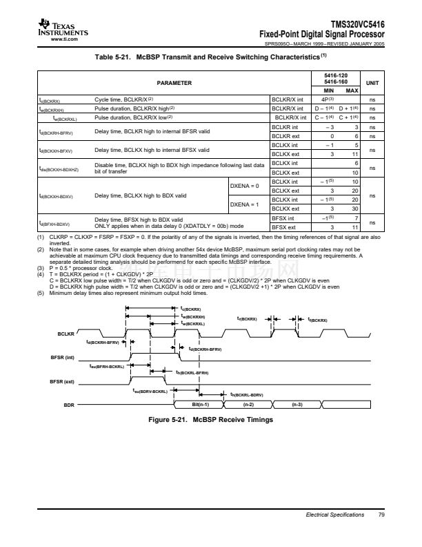
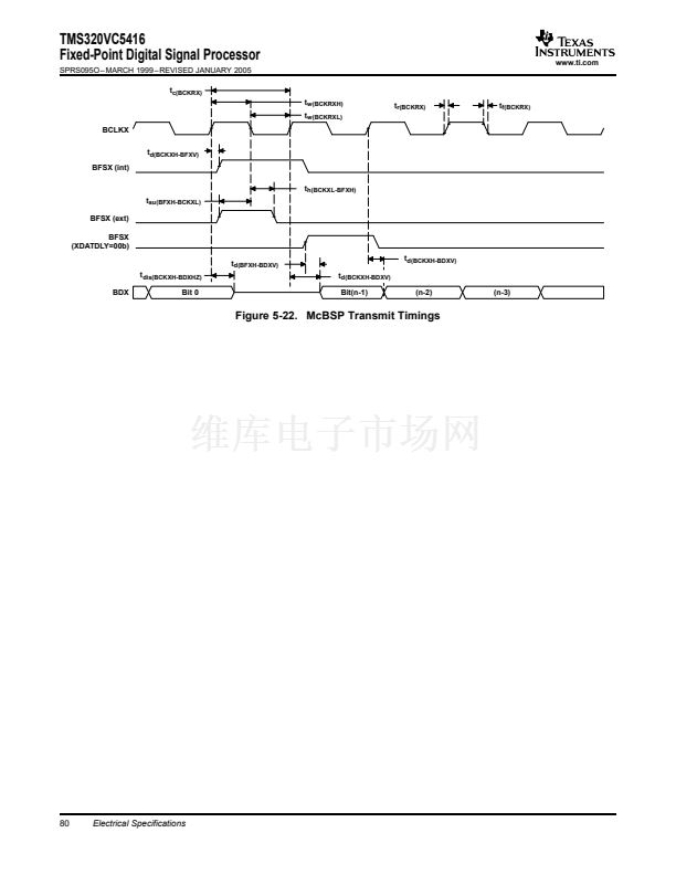
Figure 5-24. McBSP Timing as SPI Master or Slave: CLKSTP = 10b, CLKXP = 0
82
Electrical Specifications


 1
1
 2
2
 3
3
 4
4
 5
5
 6
6
 7
7
 8
8
 9
9
 10
10
 11
11
 12
12
 13
13
 14
14
 15
15
 16
16
 17
17
 18
18
 19
19
 20
20
 21
21
 22
22
 23
23
 24
24
 25
25
 26
26
 27
27
 28
28
 29
29
 30
30
 31
31
 32
32
 33
33
 34
34
 35
35
 36
36
 37
37
 38
38
 39
39
 40
40
 41
41
 42
42
 43
43
 44
44
 45
45
 46
46
 47
47
 48
48
 49
49
 50
50
 51
51
 52
52
 53
53
 54
54
 55
55
 56
56
 57
57
 58
58
 59
59
 60
60
 61
61
 62
62
 63
63
 64
64
 65
65
 66
66
 67
67
 68
68
 69
69
 70
70
 71
71
 72
72
 73
73
 74
74
 75
75
 76
76
 77
77
 78
78
 79
79
 80
80
 81
81
 82
82
 83
83
 84
84
 85
85
 86
86
 87
87
 88
88
 89
89
 90
90
 91
91
 92
92
 93
93
 94
94
 95
95
 96
96
 97
97
 98
98
