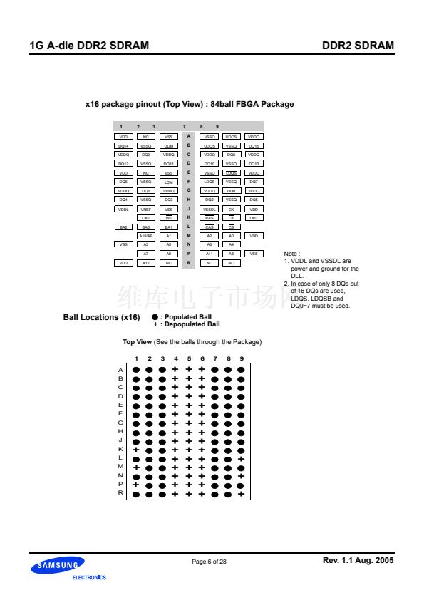
1G A-die DDR2 SDRAM
VOH + x mV
VOH + 2x mV
tHZ
tRPST end point
T2
T1
VOL + 2x mV
VOL + x mV
VTT - x mV
VTT - 2x mV
T1
T2
VTT + 2x mV
VTT + x mV
tLZ
DDR2 SDRAM
tRPRE begin point
tHZ,tRPST end point = 2*T1-T2
tLZ,tRPRE begin point = 2*T1-T2
<Test method for tLZ, tHZ, tRPRE and tRPST>
29. Input waveform timing with differential data strobe enabled MR[bit10]=0, is referenced from the input signal crossing at the V
IH(ac)
level to the differ-
ential data strobe crosspoint for a rising signal, and from the input signal crossing at the V
IL(ac)
level to the differential data strobe crosspoint for a falling
signal applied to the device under test.
30. Input waveform timing with differential data strobe enabled MR[bit10]=0, is referenced from the input signal crossing at the V
IH(dc)
level to the differ-
ential data strobe crosspoint for a rising signal and V
IL(dc)
to the differential data strobe crosspoint for a falling signal applied to the device under test.
Differential Input waveform timing
DQS
DQS
tDS
tDH
tDS
tDH
V
DDQ
V
IH(ac)
min
V
IH(dc)
min
V
REF(dc)
V
IL(dc)
max
V
IL(ac)
max
V
SS
Page 26 of 28
Rev. 1.1 Aug. 2005


 1
1
 2
2
 3
3
 4
4
 5
5
 6
6
 7
7
 8
8
 9
9
 10
10
 11
11
 12
12
 13
13
 14
14
 15
15
 16
16
 17
17
 18
18
 19
19
 20
20
 21
21
 22
22
 23
23
 24
24
 25
25
 26
26
 27
27
 28
28
