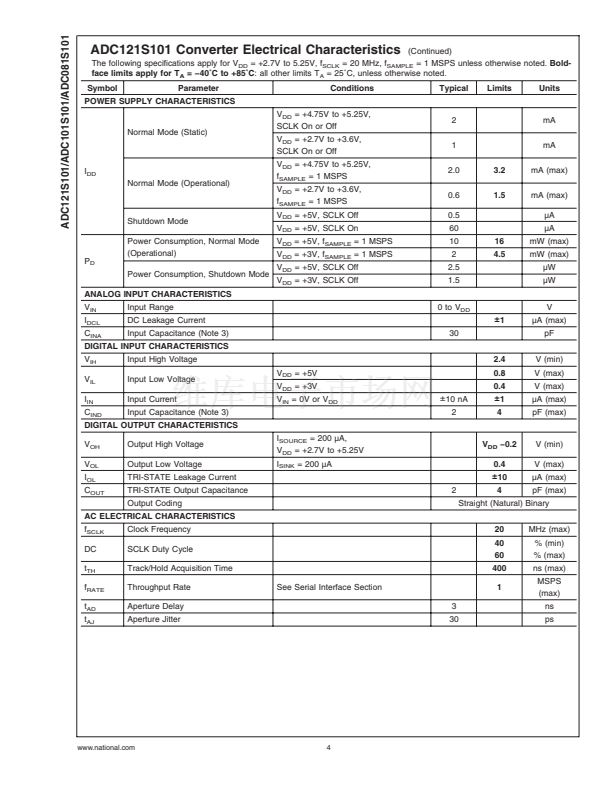
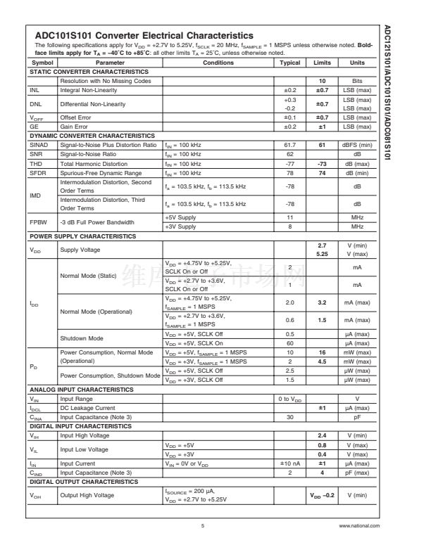
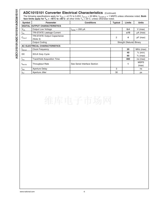
ADC121S101/ADC101S101/ADC081S101
Applications Information
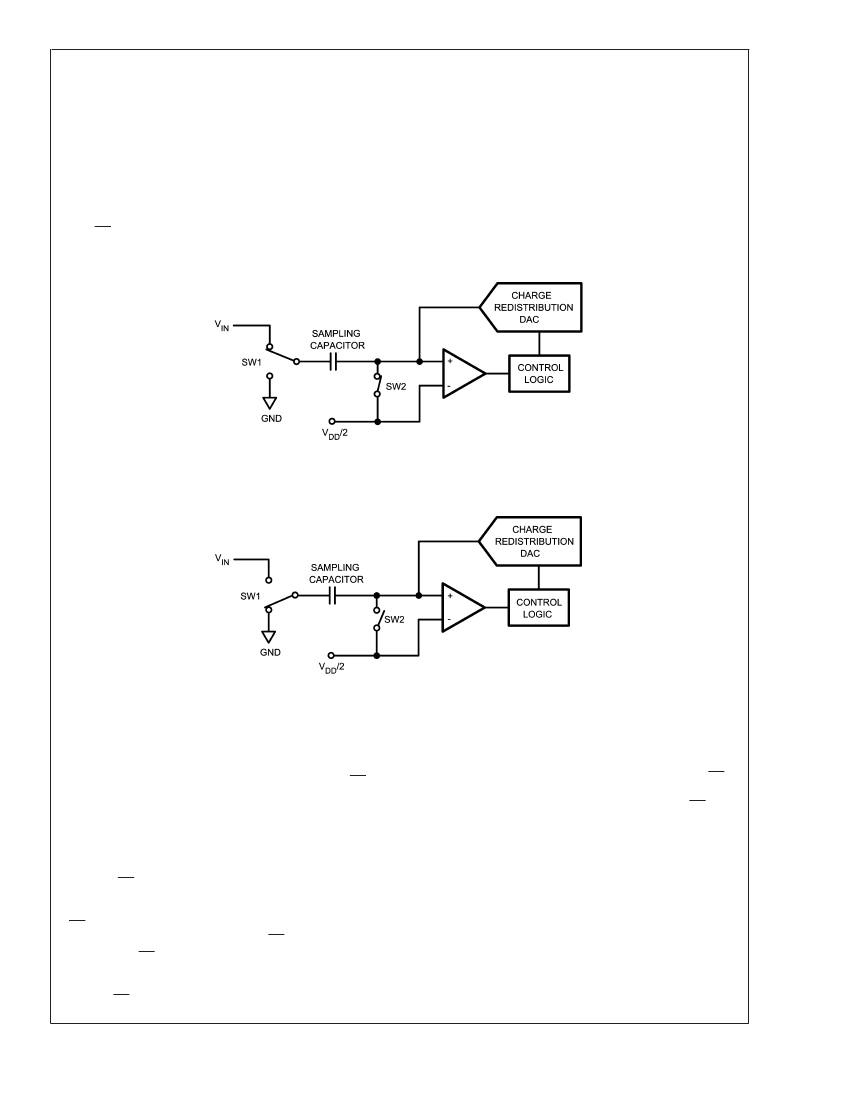
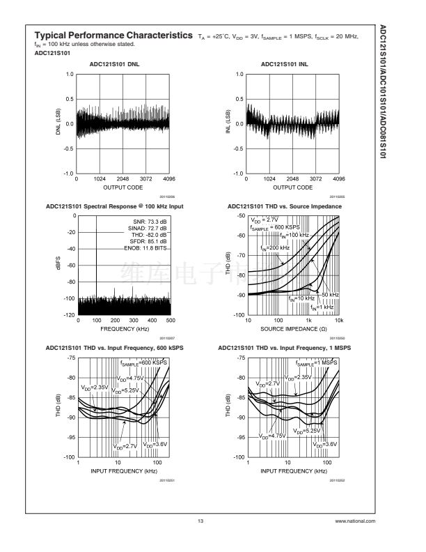
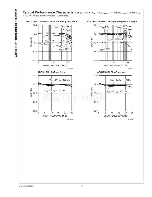
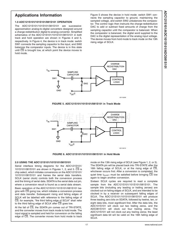
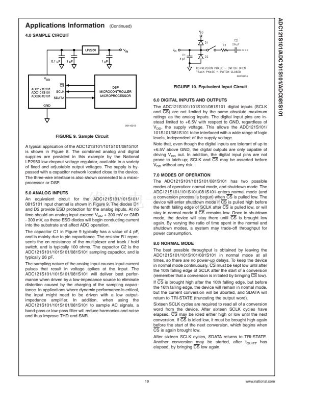
1.0 ADC121S101/101S101/081S101 OPERATION
The ADC121S101/101S101/081S101 are successive-
approximation analog-to-digital converters designed around
a charge-redistribution digital-to-analog converter. Simplified
schematics of the ADC121S101/101S101/081S101 in both
track and hold operation are shown in Figures 4 and 5,
respectively. In Figure 4, the device is in track mode: switch
SW1 connects the sampling capacitor to the input, and SW2
balances the comparator inputs. The device is in this state
until CS is brought low, at which point the device moves to
hold mode.
Figure 5 shows the device in hold mode: switch SW1 con-
nects the sampling capacitor to ground, maintaining the
sampled voltage, and switch SW2 unbalances the compara-
tor. The control logic then instructs the charge-redistribution
DAC to add or subtract fixed amounts of charge from the
sampling capacitor until the comparator is balanced. When
the comparator is balanced, the digital word supplied to the
DAC is the digital representation of the analog input voltage.
The device moves from hold mode to track mode on the 13th
rising edge of SCLK.
20110209
FIGURE 5. ADC121S101/101S101/081S101 in Track Mode
20110210
FIGURE 6. ADC121S101/101S101/081S101 in Hold Mode
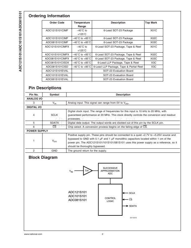
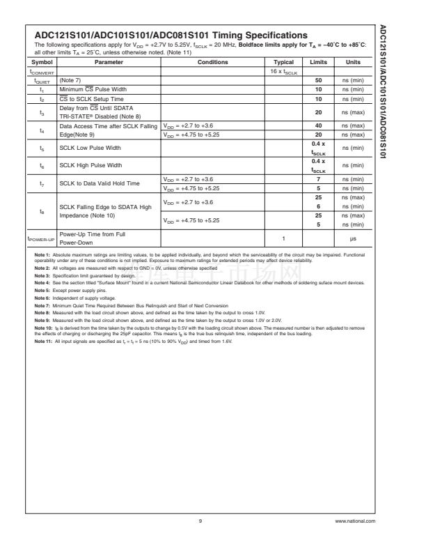
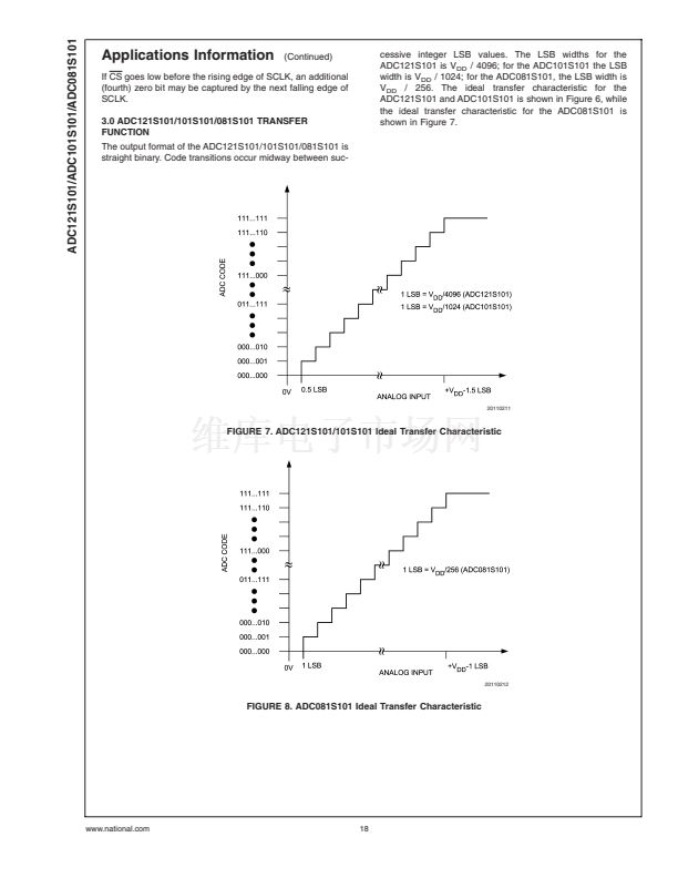
2.0 USING THE ADC121S101/101S101/081S101
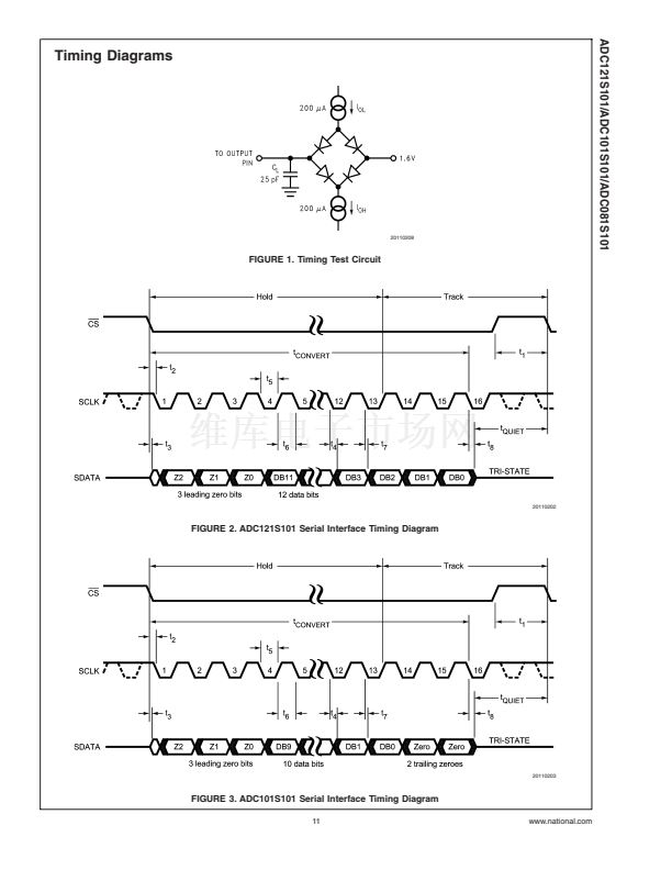
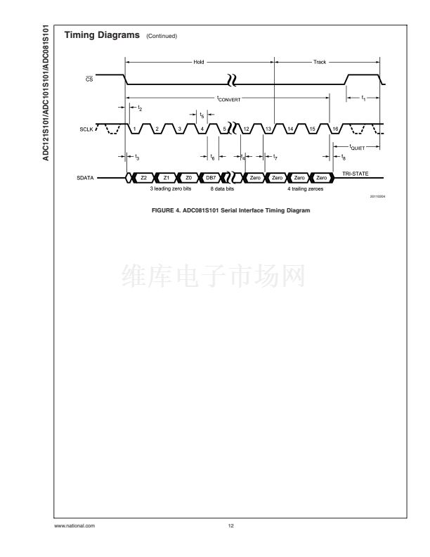
Serial interface timing diagrams for the ADC121S101/
101S101/081S101 are shown in Figures 1, 2, and 3. CS is
chip select, which initiates conversions on the ADC121S101/
101S101/081S101 and frames the serial data transfers.
SCLK (serial clock) controls both the conversion process
and the timing of serial data. SDATA is the serial data out pin,
where a conversion result is found as a serial data stream.
Basic operation of the ADC121S101/101S101/081S101 be-
gins with CS going low, which initiates a conversion process
and data transfer. Subsequent rising and falling edges of
SCLK will be labelled with reference to the falling edge of
CS; for example, "the third falling edge of SCLK" shall refer
to the third falling edge of SCLK after CS goes low.
At the fall of CS, the SDATA pin comes out of TRI-STATE,
and the converter moves from track mode to hold mode. The
input signal is sampled and held for conversion on the falling
edge of CS. The converter moves from hold mode to track
17
mode on the 13th rising edge of SCLK (see Figure 1, 2, or 3).
The SDATA pin will be placed back into TRI-STATE after the
16th falling edge of SCLK, or at the rising edge of CS,
whichever occurs first. After a conversion is completed, the
quiet time t
QUIET
must be satisfied before bringing CS low
again to begin another conversion.
Sixteen SCLK cycles are required to read a complete
sample from the ADC121S101/101S101/081S101. The
sample bits (including any leading or trailing zeroes) are
clocked out on falling edges of SCLK, and are intended to be
clocked in by a receiver on subsequent falling edges of
SCLK. The ADC121S101/101S101/081S101 will produce
three leading zero bits on SDATA, followed by twelve, ten, or
eight data bits, most significant first. After the data bits, the
ADC101S101 will clock out two trailing zeros, and the
ADC081S101 will clock out four trailing zeros. The
ADC121S101 will not clock out any trailing zeros; the least
significant data bit will be valid on the 16th falling edge of
SCLK.
www.national.com


 1
1
 2
2
 3
3
 4
4
 5
5
 6
6
 7
7
 8
8
 9
9
 10
10
 11
11
 12
12
 13
13
 14
14
 15
15
 16
16
 17
17
 18
18
 19
19
 20
20
 21
21
 22
22
 23
23
