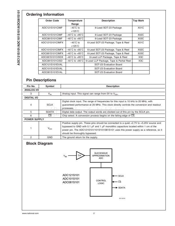
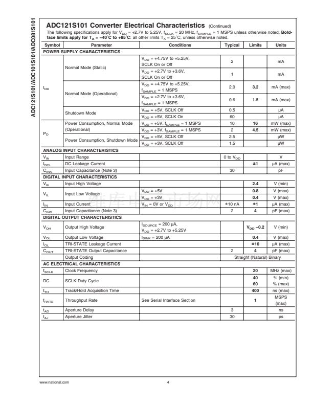
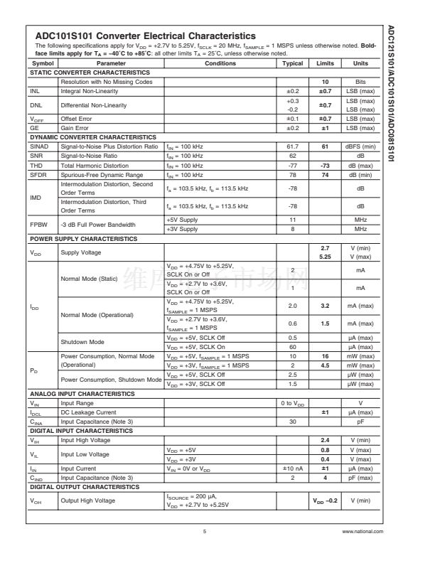
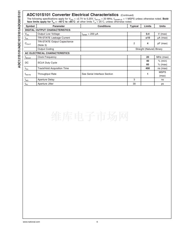
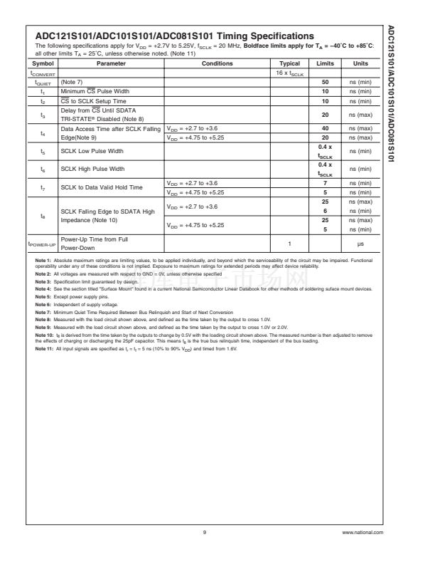
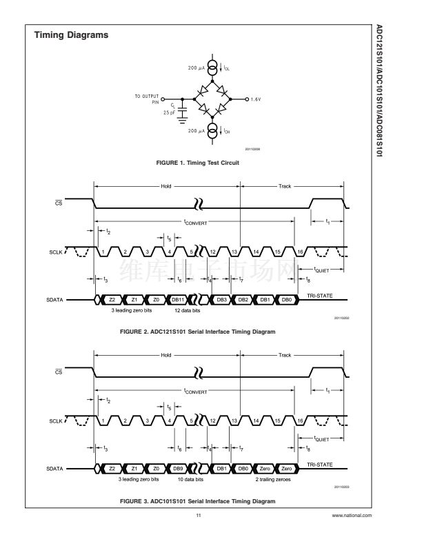
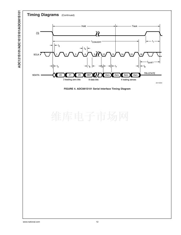
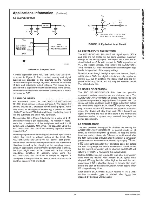
ADC121S101/ADC101S101/ADC081S101
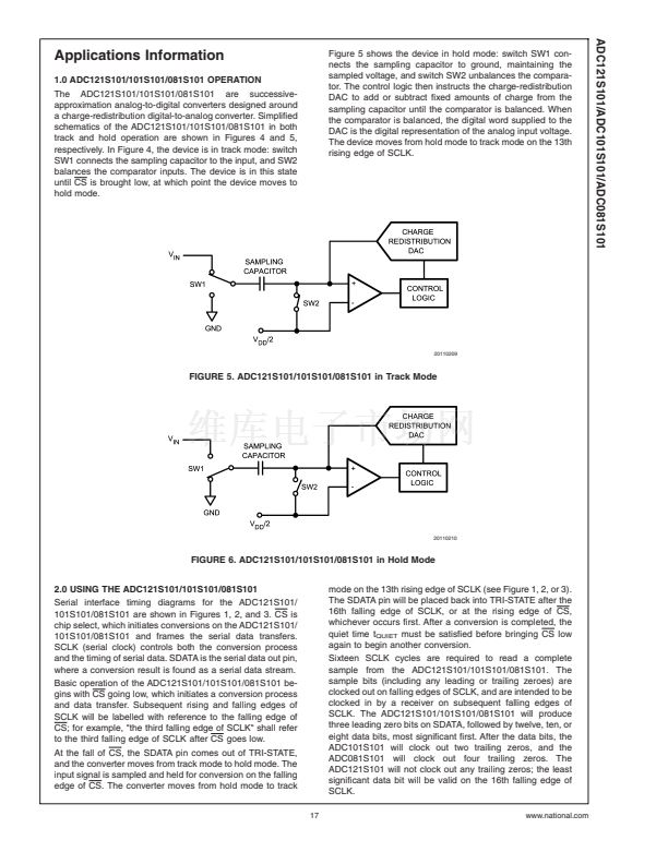
Applications Information
9.0 SHUTDOWN MODE
(Continued)
Shutdown mode is appropriate for applications that either do
not sample continuously, or are willing to trade throughput
for power consumption. When the ADC121S101/101S101/
081S101 is in shutdown mode, all of the analog circuitry is
turned off.
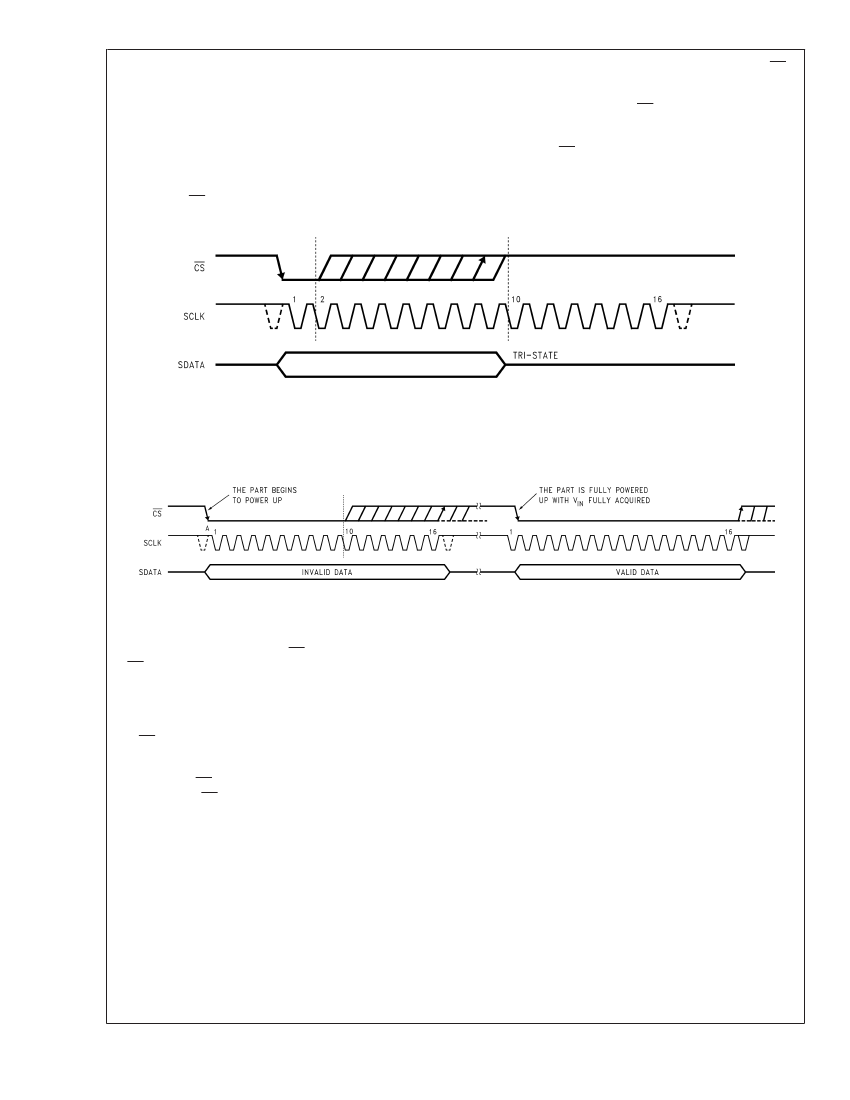
To enter shutdown mode, a conversion must be interrupted
by bringing CS back high anytime between the second and
tenth falling edges of SCLK, as shown in Figure 10. Once CS
has been brought high in this manner, the device will enter
shutdown mode; the current conversion will be aborted and
SDATA will enter TRI-STATE. If CS is brought high before the
second falling edge of SCLK, the device will not change
mode; this is to avoid accidentally changing mode as a result
of noise on the CS line.
20110216
FIGURE 11. Entering Shutdown Mode
10.0 EXITING SHUTDOWN MODE
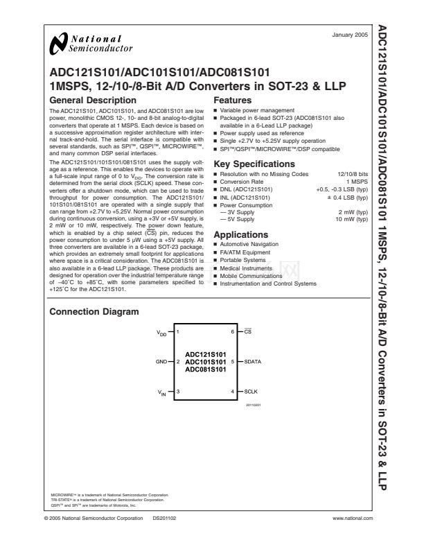
20110217
FIGURE 12. Entering Normal Mode
To exit shutdown mode, bring CS back low. Upon bringing
CS low, the ADC121S101/101S101/081S101 will begin pow-
ering up. Power up typically takes 1 碌s. This microsecond of
power-up delay results in the first conversion result being
unusable. The second conversion performed after power-up,
however, is valid, as shown in Figure 11.
If CS is brought back high before the 10th falling edge of
SCLK, the device will return to shutdown mode. This is done
to avoid accidentally entering normal mode as a result of
noise on the CS line. To exit shutdown mode and remain in
normal mode, CS must be kept low until after the 10th falling
edge of SCLK. The ADC121S101/101S101/081S101 will be
fully powered-up after 16 SCLK cycles.
11.0 POWER-UP TIMING
The ADC121S101/101S101/081S101 typically requires 1 碌s
to power up, either after first applying V
DD
, or after returning
to normal mode from shutdown mode. This corresponds to
one "dummy" conversion for any SCLK frequency within the
specifications in this document. After this first dummy con-
version, the ADC121S101/101S101/081S101 will perform
conversions properly. Note that the t
QUIET
time must still be
included between the first dummy conversion and the sec-
ond valid conversion.
12.0 STARTUP MODE
When the V
DD
supply is first applied, the ADC121S101/
101S101/081S101 may power up in either of the two modes:
normal or shutdown. As such, one dummy conversion
should be performed after start-up, exactly as described in
Section 11.0. The part may then be placed into either normal
mode or the shutdown mode, as described in Sections 8.0
and 9.0.
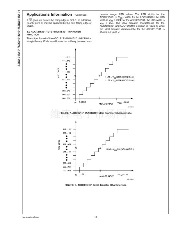
13.0 POWER MANAGEMENT
When the ADC121S101/101S101/081S101 is operated con-
tinuously in normal mode, throughput up to 1 MSPS can be
achieved. The user may trade throughput for power con-
sumption by simply performing fewer conversions per unit
time, and putting the ADC121S101/101S101/081S101 into
shutdown mode between conversions. This method is not
advantageous beyond 350 kSPS throughput.
A plot of maximum power consumption versus throughput is
shown in Figure 12 below. To calculate the power consump-
tion for a given throughput, remember that each time the part
exits shutdown mode and enters normal mode, one dummy
conversion is required. Generally, the user will put the part
into normal mode, execute one dummy conversion followed
by one valid conversion, and then put the part back into
shutdown mode. When this is done, the fraction of time
20
www.national.com


 1
1
 2
2
 3
3
 4
4
 5
5
 6
6
 7
7
 8
8
 9
9
 10
10
 11
11
 12
12
 13
13
 14
14
 15
15
 16
16
 17
17
 18
18
 19
19
 20
20
 21
21
 22
22
 23
23
