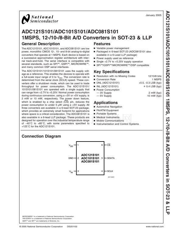
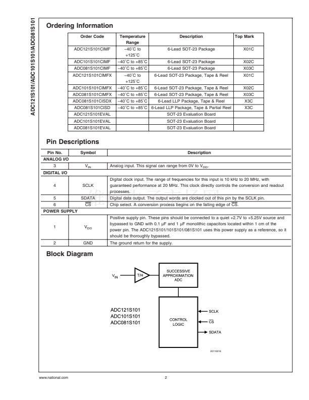
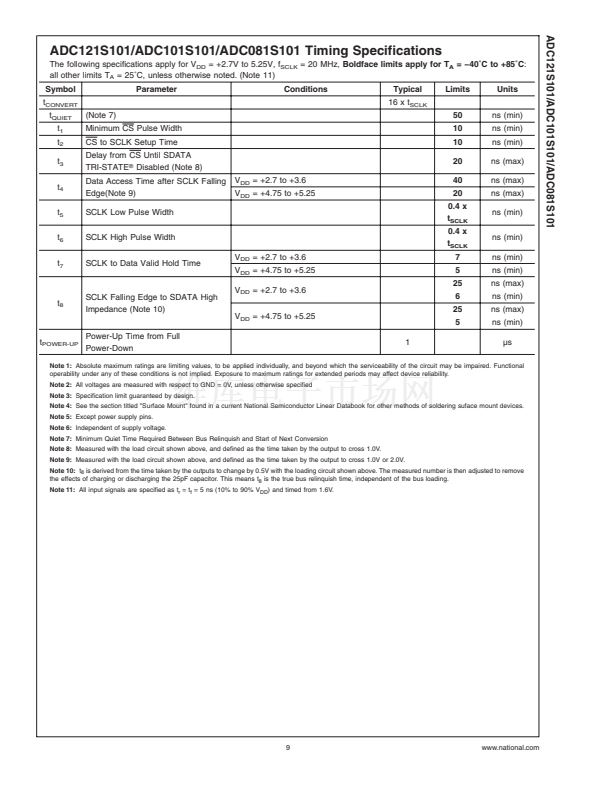
ADC121S101/ADC101S101/ADC081S101
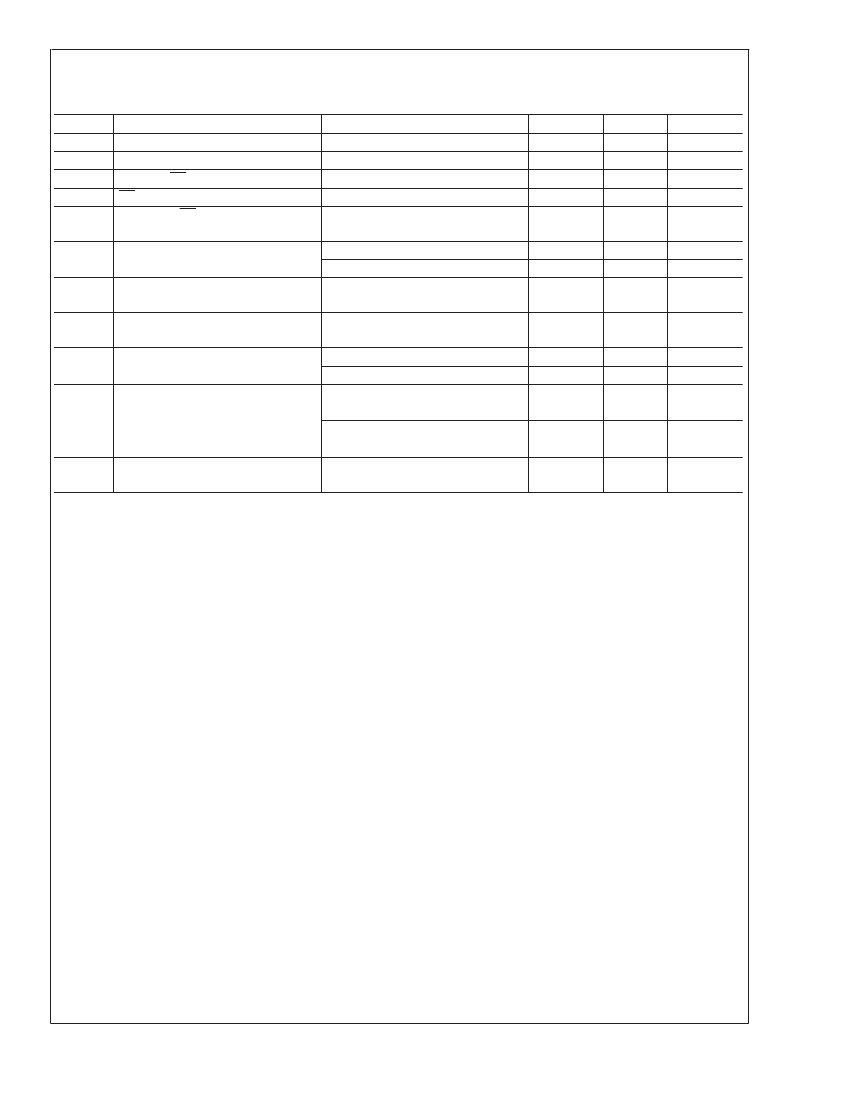
ADC121S101/ADC101S101/ADC081S101 Timing Specifications
The following specifications apply for V
DD
= +2.7V to 5.25V, f
SCLK
= 20 MHz,
Boldface limits apply for T
A
= 鈭?0藲C to +85藲C:
all other limits T
A
= 25藲C, unless otherwise noted. (Note 11)
Symbol
t
CONVERT
t
QUIET
t
1
t
2
t
3
t
4
t
5
t
6
t
7
(Note 7)
Minimum CS Pulse Width
CS to SCLK Setup Time
Delay from CS Until SDATA
TRI-STATE
庐
Disabled (Note 8)
Data Access Time after SCLK Falling
Edge(Note 9)
SCLK Low Pulse Width
SCLK High Pulse Width
SCLK to Data Valid Hold Time
V
DD
= +2.7 to +3.6
V
DD
= +4.75 to +5.25
V
DD
= +2.7 to +3.6
V
DD
= +4.75 to +5.25
1
V
DD
= +2.7 to +3.6
V
DD
= +4.75 to +5.25
Parameter
Conditions
Typical
16 x t
SCLK
50
10
10
20
40
20
0.4 x
t
SCLK
0.4 x
t
SCLK
7
5
25
6
25
5
ns (min)
ns (min)
ns (min)
ns (max)
ns (max)
ns (max)
ns (min)
ns (min)
ns (min)
ns (min)
ns (max)
ns (min)
ns (max)
ns (min)
碌s
Limits
Units
t
8
SCLK Falling Edge to SDATA High
Impedance (Note 10)
Power-Up Time from Full
Power-Down
t
POWER-UP
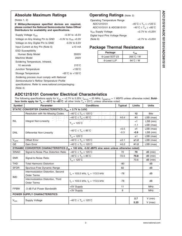
Note 1:
Absolute maximum ratings are limiting values, to be applied individually, and beyond which the serviceability of the circuit may be impaired. Functional
operability under any of these conditions is not implied. Exposure to maximum ratings for extended periods may affect device reliability.
Note 2:
All voltages are measured with respect to GND = 0V, unless otherwise specified
Note 3:
Specification limit guaranteed by design.
Note 4:
See the section titled "Surface Mount" found in a current National Semiconductor Linear Databook for other methods of soldering suface mount devices.
Note 5:
Except power supply pins.
Note 6:
Independent of supply voltage.
Note 7:
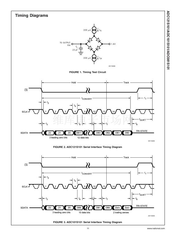
Minimum Quiet Time Required Between Bus Relinquish and Start of Next Conversion
Note 8:
Measured with the load circuit shown above, and defined as the time taken by the output to cross 1.0V.
Note 9:
Measured with the load circuit shown above, and defined as the time taken by the output to cross 1.0V or 2.0V.
Note 10:
t
8
is derived from the time taken by the outputs to change by 0.5V with the loading circuit shown above. The measured number is then adjusted to remove
the effects of charging or discharging the 25pF capacitor. This means t
8
is the true bus relinquish time, independent of the bus loading.
Note 11:
All input signals are specified as t
r
= t
f
= 5 ns (10% to 90% V
DD
) and timed from 1.6V.
9
www.national.com


 1
1
 2
2
 3
3
 4
4
 5
5
 6
6
 7
7
 8
8
 9
9
 10
10
 11
11
 12
12
 13
13
 14
14
 15
15
 16
16
 17
17
 18
18
 19
19
 20
20
 21
21
 22
22
 23
23
