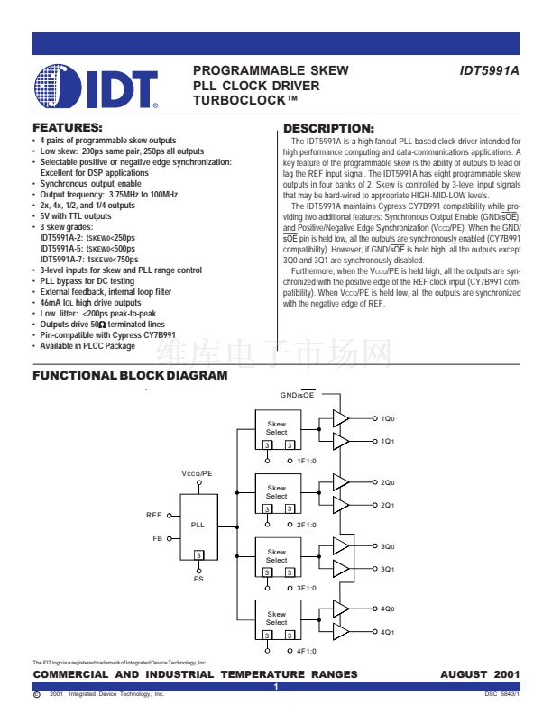
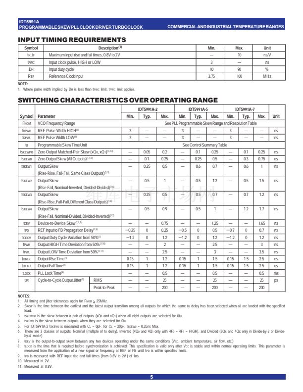
IDT5991A
PROGRAMMABLE SKEW PLL CLOCK DRIVER TURBOCLOCK
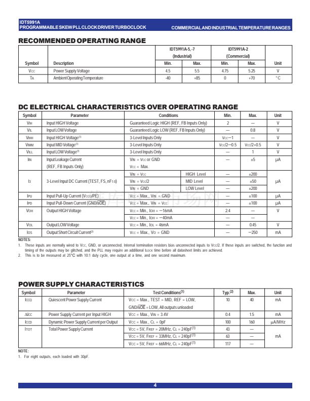
COMMERCIAL AND INDUSTRIAL TEMPERATURE RANGES
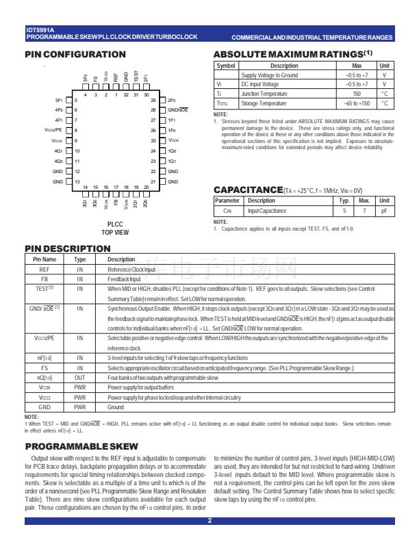
PIN CONFIGURATION
TEST
V
CCQ
GND
3F
0
REF
2F
1
FS
ABSOLUTE MAXIMUM RATINGS
(1)
Symbol
V
I
T
J
29
28
27
26
25
24
23
22
21
2F
0
GND/sOE
1F
1
1F
0
V
CCN
1Q
0
1Q
1
GND
GND
Description
Supply Voltage to Ground
DC Input Voltage
Junction Temperature
Storage Temperature
Max
鈥?.5 to +7
鈥?.5 to +7
150
鈥?5 to +150
Unit
V
V
掳C
掳C
4
3F
1
4F
0
4F
1
V
CCQ
/PE
V
CCN
4Q
1
4Q
0
GND
GND
5
6
7
8
9
10
11
12
13
14
3
2
1
32
31
30
T
STG
NOTE:
1. Stresses beyond those listed under ABSOLUTE MAXIMUM RATINGS may cause
permanent damage to the device. These are stress ratings only, and functional
operation of the device at these or any other conditions above those indicated in the
operational sections of this specification is not implied. Exposure to absolute-
maximum-rated conditions for extended periods may affect device reliability.
15
16
17
18
19
20
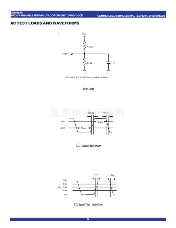
CAPACITANCE
(T
A
= +25掳C, f = 1MHz, V
IN
= 0V)
Parameter
C
IN
Description
Input Capacitance
Typ.
5
Max.
7
Unit
pF
V
CCN
V
CCN
3Q
0
3Q
1
FB
2Q
1
2Q
0
PLCC
TOP VIEW
NOTE:
1. Capacitance applies to all inputs except TEST, FS, and nF1:0.
PIN DESCRIPTION
Pin Name
REF
FB
TEST
(1)
GND/
sOE
(1)
Type
IN
IN
IN
IN
Description
Reference Clock Input
Feedback Input
When MID or HIGH, disables PLL (except for conditions of Note 1). REF goes to all outputs. Skew selections (see Control
Summary Table) remain in effect. Set LOW for normal operation.
Synchronous Output Enable. When HIGH, it stops clock outputs (except 3Q
0
and 3Q
1
) in a LOW state - 3Q
0
and 3Q
1
may be used as
the feedback signal to maintain phase lock. When TEST is held at MID level and GND/sOE is HIGH, the nF[
1:0
] pins act as output disable
controls for individual banks when nF[
1:0
] = LL. Set GND/sOE LOW for normal operation.
V
CCQ
/PE
nF[
1:0
]
FS
nQ[
1:0
]
V
CCN
V
CCQ
GND
IN
IN
IN
OUT
PWR
PWR
PWR
Selectable positive or negative edge control. When LOW/HIGH the outputs are synchronized with the negative/positive edge of the
reference clock.
3-level inputs for selecting 1 of 9 skew taps or frequency functions
Selects appropriate oscillator circuit based on anticipated frequency range. (See PLL Programmable Skew Range.)
Four banks of two outputs with programmable skew
Power supply for output buffers
Power supply for phase locked loop and other internal circuitry
Ground
NOTE:
1.When TEST = MID and GND/sOE = HIGH, PLL remains active with nF[
1:0
] = LL functioning as an output disable control for individual output banks. Skew selections remain
in effect unless nF[
1:0
] = LL.
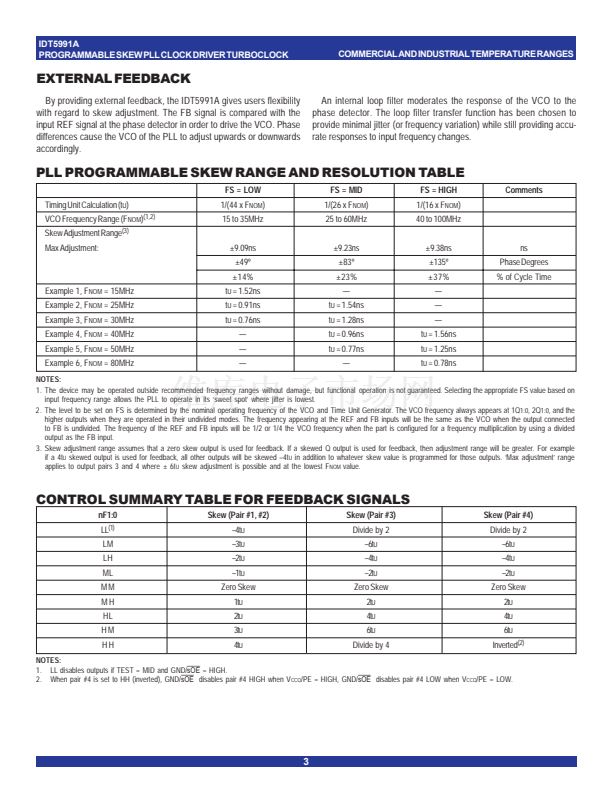
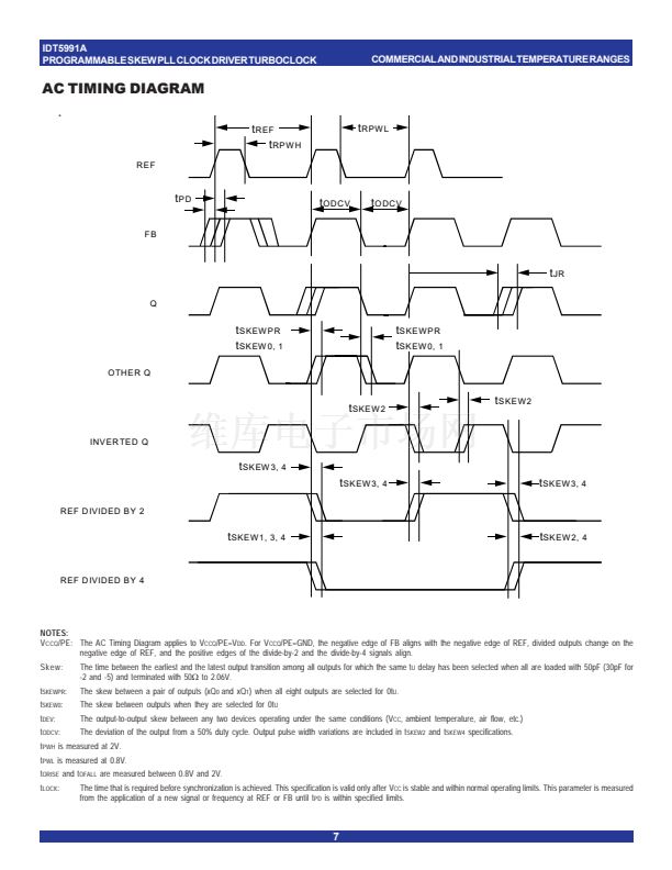
PROGRAMMABLE SKEW
Output skew with respect to the REF input is adjustable to compensate
for PCB trace delays, backplane propagation delays or to accommodate
requirements for special timing relationships between clocked compo-
nents. Skew is selectable as a multiple of a time unit t
U
which is of the
order of a nanosecond (see PLL Programmable Skew Range and Resolution
Table). There are nine skew configurations available for each output
pair. These configurations are chosen by the nF
1:0
control pins. In order
2
to minimize the number of control pins, 3-level inputs (HIGH-MID-LOW)
are used, they are intended for but not restricted to hard-wiring. Undriven
3-level inputs default to the MID level. Where programmable skew is
not a requirement, the control pins can be left open for the zero skew
default setting. The Control Summary Table shows how to select specific
skew taps by using the nF
1:0
control pins.


 1
1
 2
2
 3
3
 4
4
 5
5
 6
6
 7
7
 8
8
