S6B1713
65 COM / 132 SEG DRIVER & CONTROLLER FOR STN LCD
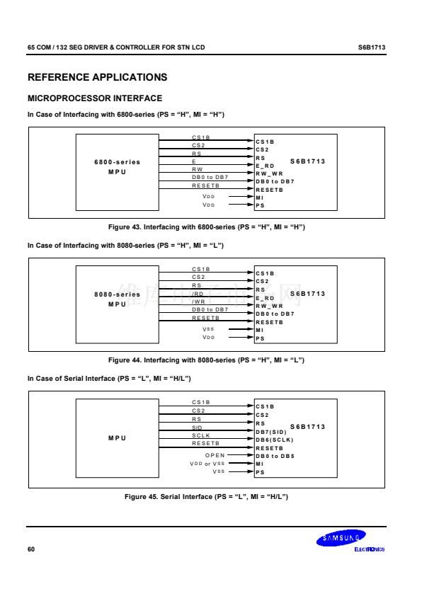
MICROPROCESSOR INTERFACE
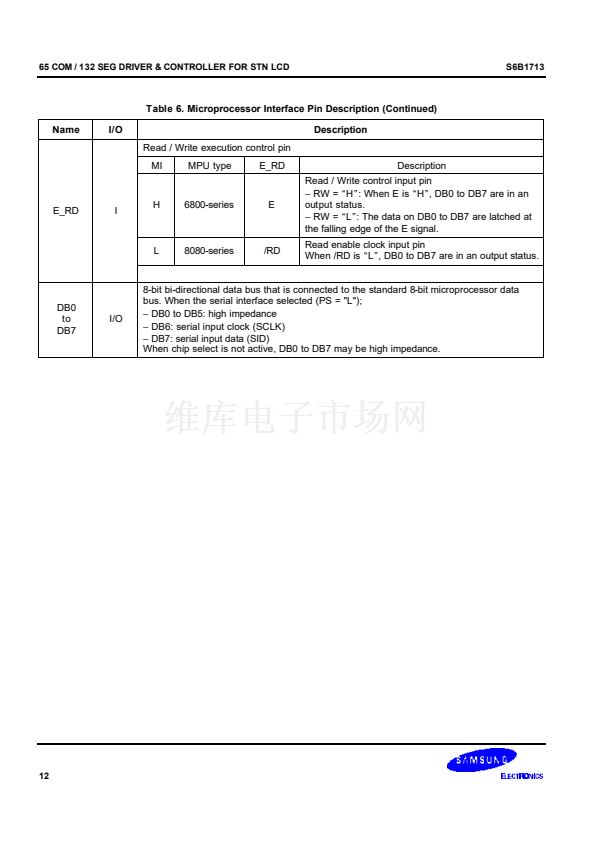
Table 6. Microprocessor Interface Pin Description
Name
RESETB
I/O
I
Description
Reset input pin
When RESETB is 鈥淟鈥? initialization is executed.
Parallel / Serial data input select input
PS
H
L
Interface
mode
Parallel
Serial
Chip
select
CS1B,
CS2
CS1B,
CS2
Data /
instruction
RS
RS
Data
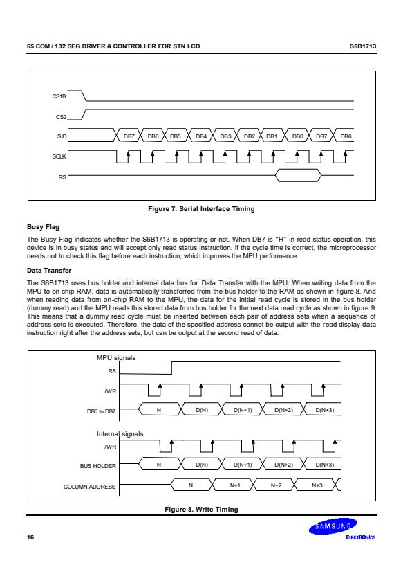
DB0 to DB7
SID(DB7)
Read / Write
E_RD
RW_WR
Write only
Serial clock
-
SCLK(DB6)
PS
I
*NOTE: In serial mode, it is impossible to read data from the on-chip RAM. And DB0 to DB5
are high impedance and E_RD and RW_WR must be fixed to either 鈥淗鈥?or 鈥淟鈥?
MI
CS1B
CS2
RS
I
Microprocessor interface selects input pin
鈭?/div>
MI = "H": 6800-series MPU interface
鈭?/div>
MI = "L": 8080-series MPU interface
Chip select input pins
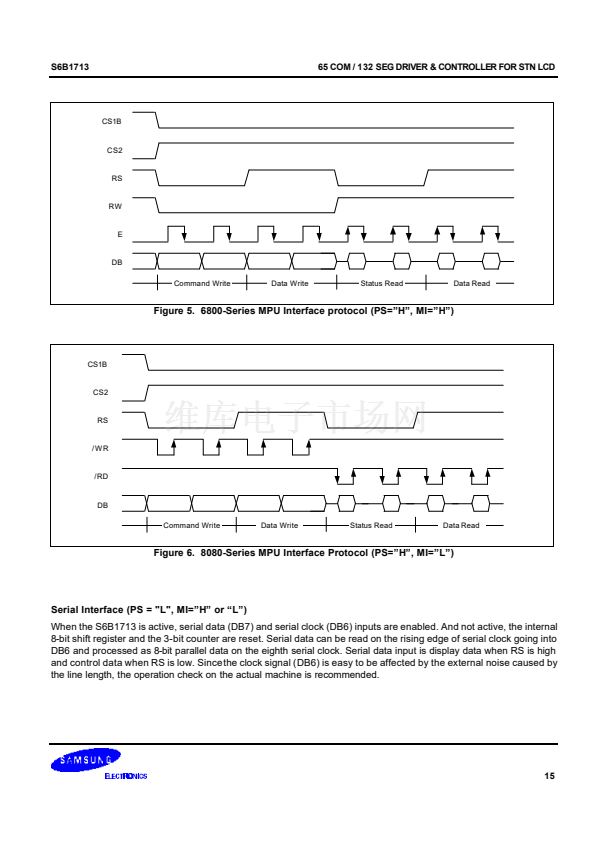
Data / instruction I/O is enabled only when CS1B is 鈥淟鈥?and CS2 is 鈥淗鈥?
When chip select is non-active, DB0 to DB7 may be high impedance.
Register select input pin
鈭?/div>
RS = "H": DB0 to DB7 are display data
鈭?/div>
RS = "L": DB0 to DB7 are control data
Read / Write execution control pin
MI
H
RW_WR
I
L
8080-series
/WR
MPU type
6800-series
RW_WR
RW
Description
Read / Write control input pin
鈭?/div>
RW = 鈥淗鈥? read
鈭?/div>
RW = 鈥淟鈥? write
Write enable clock input pin
The data ON DB0 to DB7 are latched at the rising
edge of the /WR signal.
I
I
11
S6B1713A15-B0CZ相关型号PDF文件下载
-
型号
版本
描述
厂商
下载
-
英文版
65 COM / 132 SEG DRIVER & CONTROLLER FOR STN LCD
SAMSUNG [S...
-
英文版
128 SEG / 129 COM DRIVER & CONTROLLER FOR 4 GRAY SCALE STN L...
-
英文版
128 SEG / 129 COM DRIVER & CONTROLLER FOR 4 GRAY SCALE STN L...
SAMSUNG [S...
-
英文版
Mobile DDI
-
英文版
Mobile DDI
-
英文版
65 COM / 132 SEG DRIVER & CONTROLLER FOR STN LCD
-
英文版
65 COM / 132 SEG DRIVER & CONTROLLER FOR STN LCD
SAMSUNG [S...
-
英文版
65 COM / 132 SEG DRIVER & CONTROLLER FOR STN LCD
-
英文版
65 COM / 132 SEG DRIVER & CONTROLLER FOR STN LCD
SAMSUNG [S...
-
英文版
65 COM / 132 SEG DRIVER & CONTROLLER FOR STN LCD
-
英文版
65 COM / 132 SEG DRIVER & CONTROLLER FOR STN LCD
SAMSUNG [S...
-
英文版
65 COM / 132 SEG DRIVER & CONTROLLER FOR STN LCD
-
英文版
65 COM / 132 SEG DRIVER & CONTROLLER FOR STN LCD
SAMSUNG [S...
-
英文版
65 COM / 132 SEG DRIVER & CONTROLLER FOR STN LCD
-
英文版
65 COM / 132 SEG DRIVER & CONTROLLER FOR STN LCD
SAMSUNG [S...
-
英文版
65 COM / 132 SEG DRIVER & CONTROLLER FOR STN LCD
-
英文版
65 COM / 132 SEG DRIVER & CONTROLLER FOR STN LCD
SAMSUNG [S...
-
英文版
65 COM / 132 SEG DRIVER & CONTROLLER FOR STN LCD
-
英文版
65 COM / 132 SEG DRIVER & CONTROLLER FOR STN LCD
SAMSUNG [S...
-
英文版
65 COM / 132 SEG DRIVER & CONTROLLER FOR STN LCD


 1
1
 2
2
 3
3
 4
4
 5
5
 6
6
 7
7
 8
8
 9
9
 10
10
 11
11
 12
12
 13
13
 14
14
 15
15
 16
16
 17
17
 18
18
 19
19
 20
20
 21
21
 22
22
 23
23
 24
24
 25
25
 26
26
 27
27
 28
28
 29
29
 30
30
 31
31
 32
32
 33
33
 34
34
 35
35
 36
36
 37
37
 38
38
 39
39
 40
40
 41
41
 42
42
 43
43
 44
44
 45
45
 46
46
 47
47
 48
48
 49
49
 50
50
 51
51
 52
52
 53
53
 54
54
 55
55
 56
56
 57
57
 58
58
 59
59
 60
60
 61
61
 62
62
 63
63
 64
64
 65
65
 66
66
 67
67
 68
68
 69
69
 70
70
