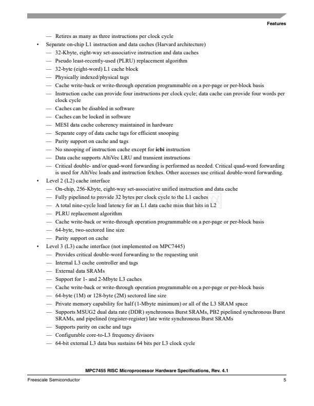
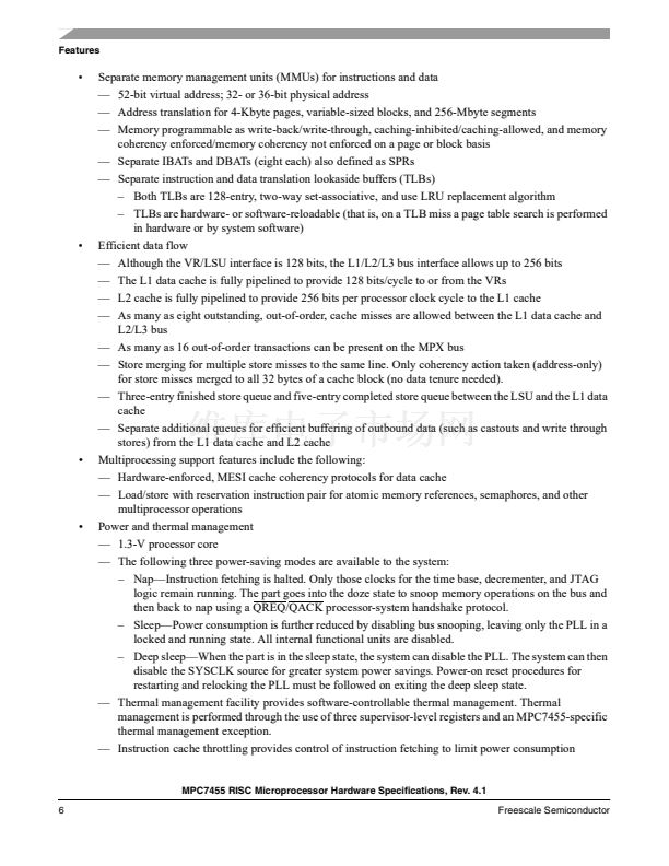
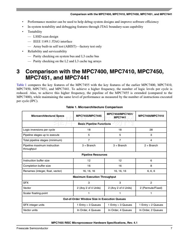
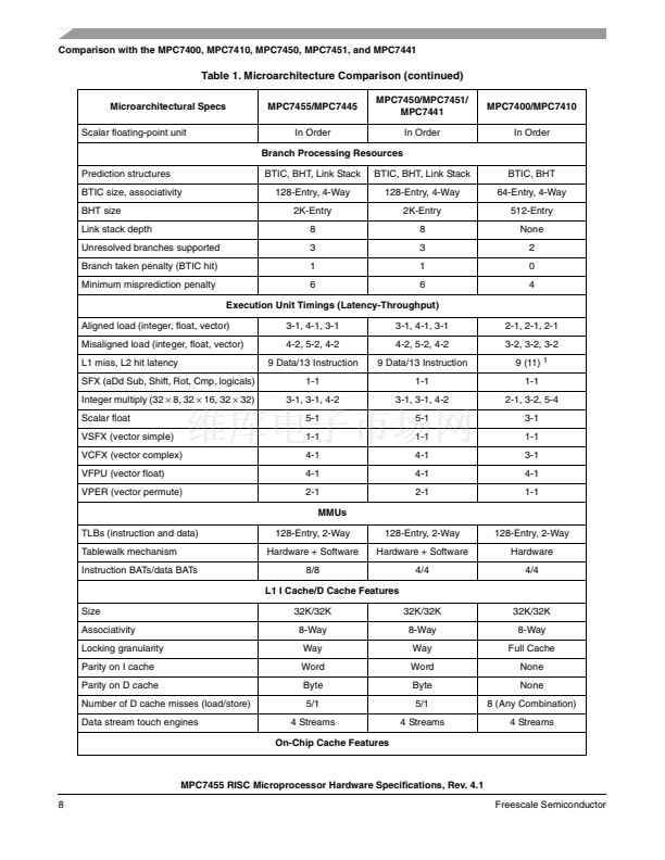
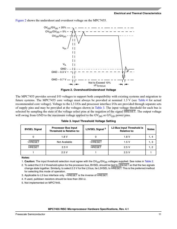
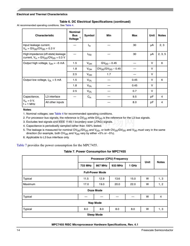
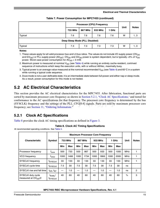
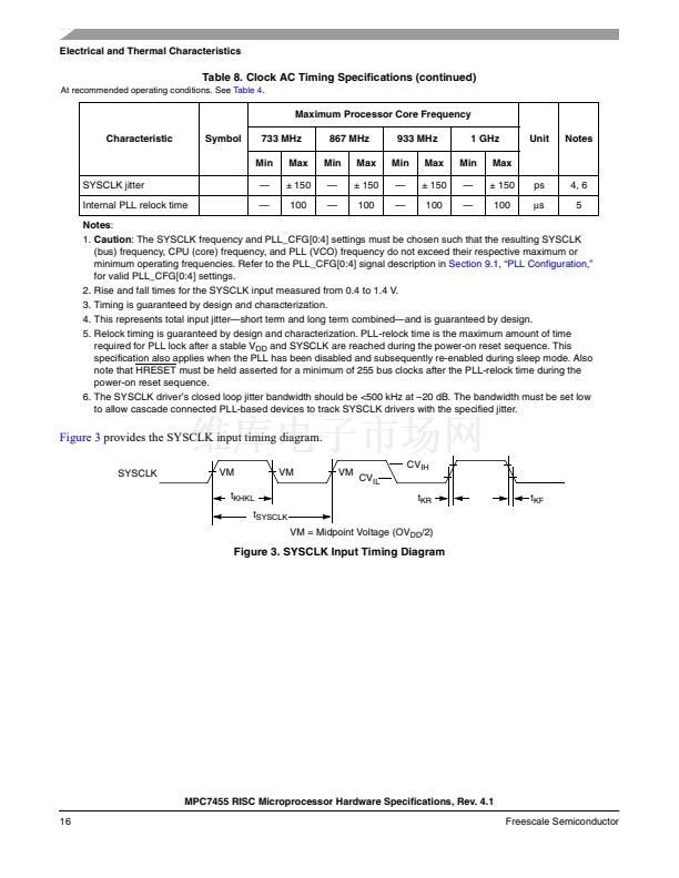
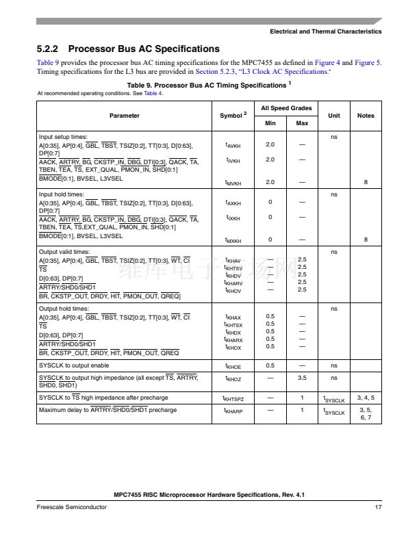
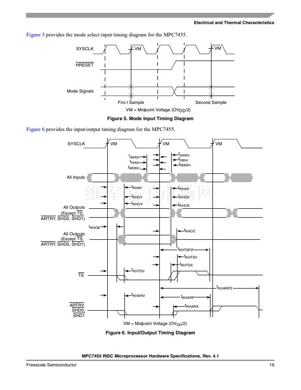
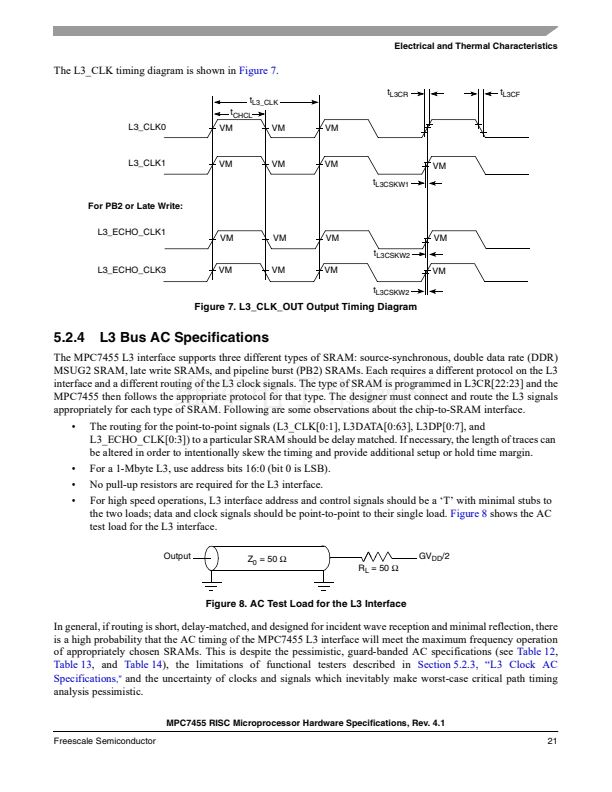
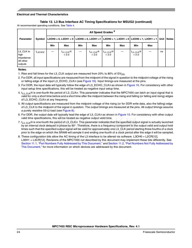
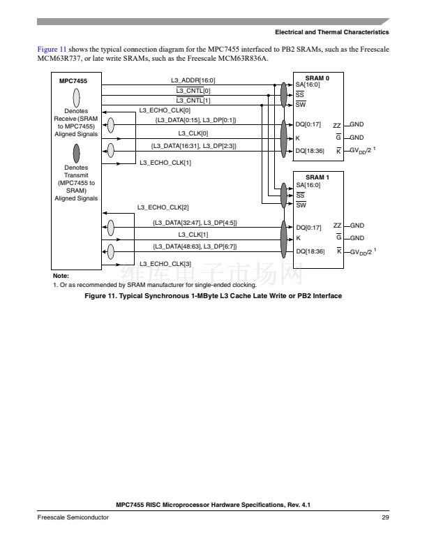
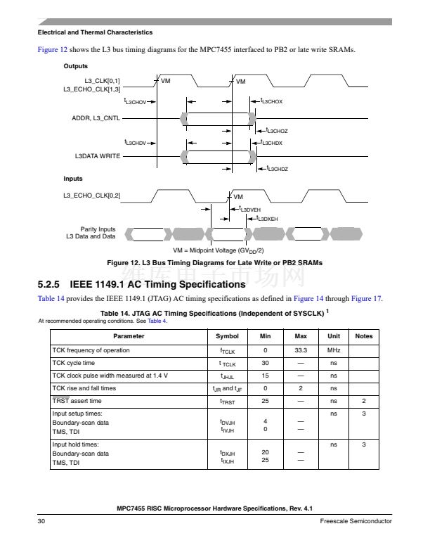
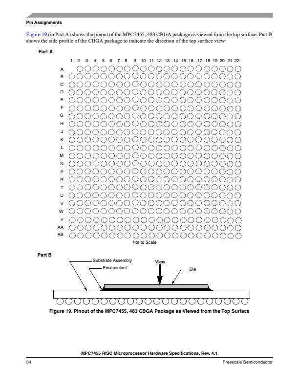
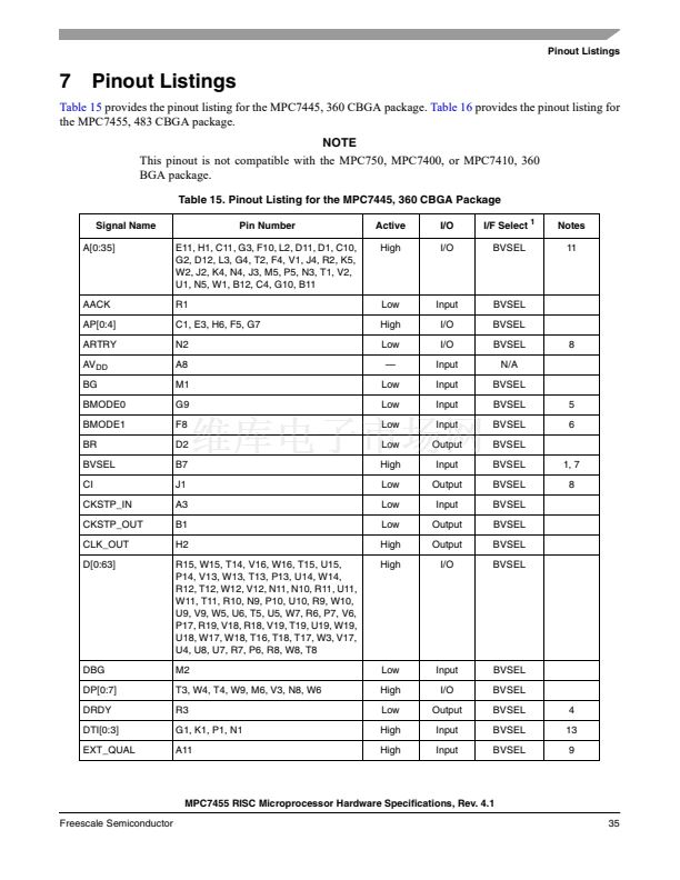
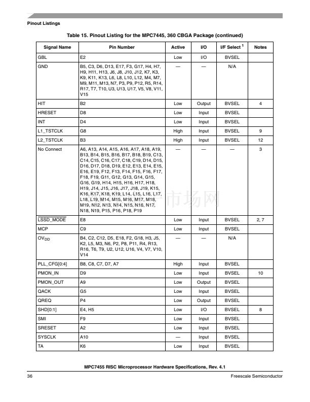
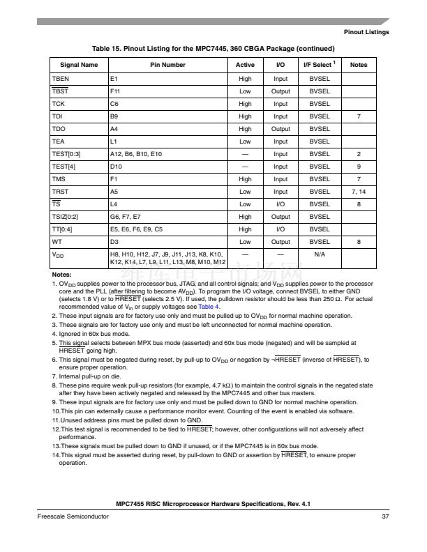
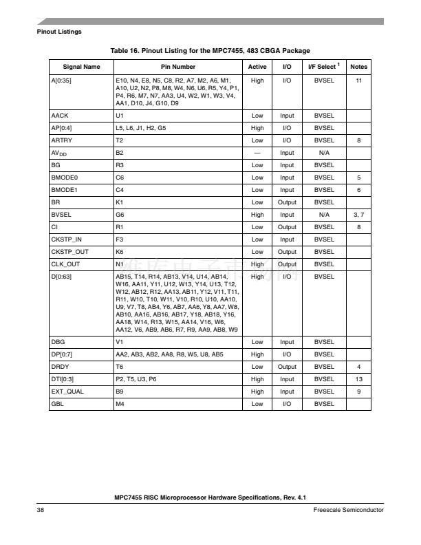
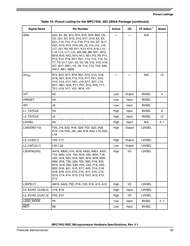
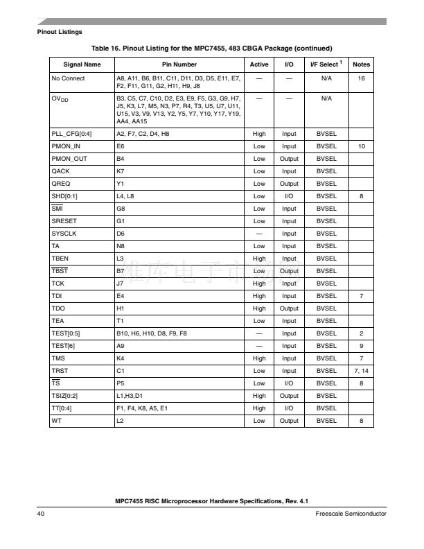
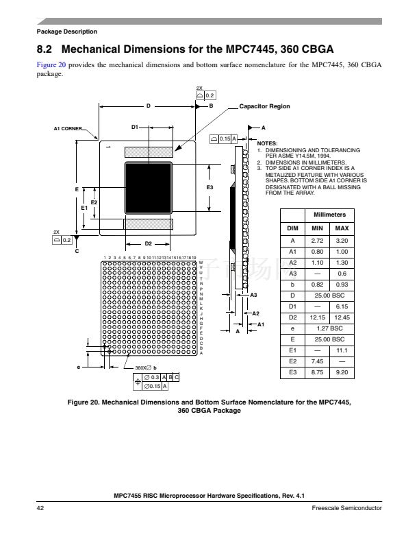
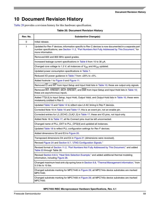
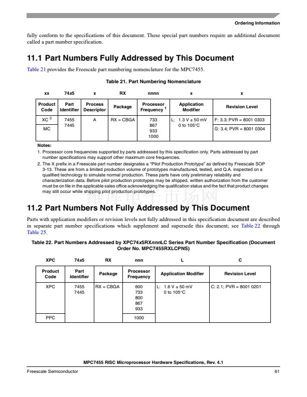
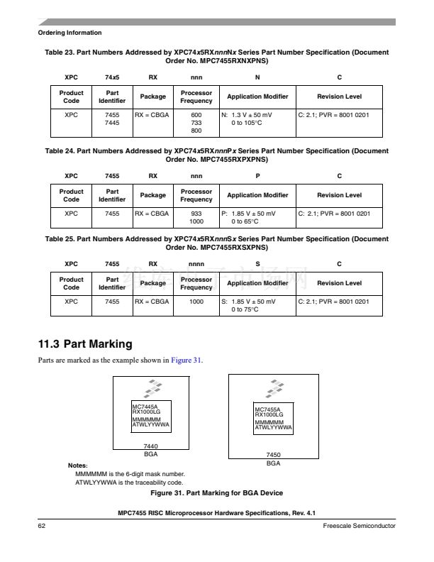
Electrical and Thermal Characteristics
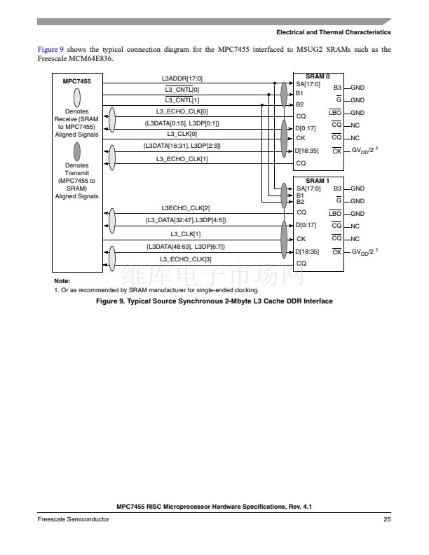
More specifically, certain signals within groups should be delay-matched with others in the same group while
intergroup routing is less critical. Only the address and control signals are common to both SRAMs and additional
timing margin is available for these signals. The double-clocked data signals are grouped with individual clocks as
shown in
Figure 9
or
Figure 11,
depending on the type of SRAM. For example, for the MSUG2 DDR SRAM (see
Figure 9);
L3DATA[0:31], L3DP[0:3], and L3_CLK[0] form a closely coupled group of outputs from the MPC7455;
while L3DATA[0:15], L3DP[0:1], and L3_ECHO_CLK[0] form a closely coupled group of inputs.
The
MPC7450 RISC Microprocessor Family User鈥檚 Manual
refers to logical settings called 鈥榮ample points鈥?used in
the synchronization of reads from the receive FIFO. The computation of the correct value for this setting is
system-dependent and is described in the
MPC7450 RISC Microprocessor Family User鈥檚 Manual.
Three
specifications are used in this calculation and are given in
Table 11.
It is essential that all three specifications are
included in the calculations to determine the sample points, as incorrect settings can result in errors and
unpredictable behavior. For more information, see the
MPC7450 RISC Microprocessor Family User鈥檚 Manual.
Table 11. Sample Points Calculation Parameters
Parameter
Delay from processor clock to internal_L3_CLK
Delay from internal_L3_CLK to L3_CLKn output pins
Delay from L3_ECHO_CLKn to receive latch
Symbol
t
AC
t
CO
t
ECI
Max
3/4
3
3
Unit
t
L3_CLK
ns
ns
Notes
1
2
3
Notes:
1. This specification describes a logical offset between the internal clock edge used to launch the L3 address and
control signals (this clock edge is phase-aligned with the processor clock edge) and the internal clock edge used to
launch the L3_CLKn signals. With proper board routing, this offset ensures that the L3_CLKn edge will arrive at the
SRAM within a valid address window and provide adequate setup and hold time. This offset is reflected in the L3
bus interface AC timing specifications, but must also be separately accounted for in the calculation of sample points
and, thus, is specified here.
2. This specification is the delay from a rising or falling edge on the internal_L3_CLK signal to the corresponding rising
or falling edge at the L3CLKn pins.
3. This specification is the delay from a rising or falling edge of L3_ECHO_CLKn to data valid and ready to be sampled
from the FIFO.
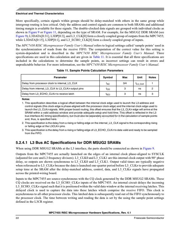
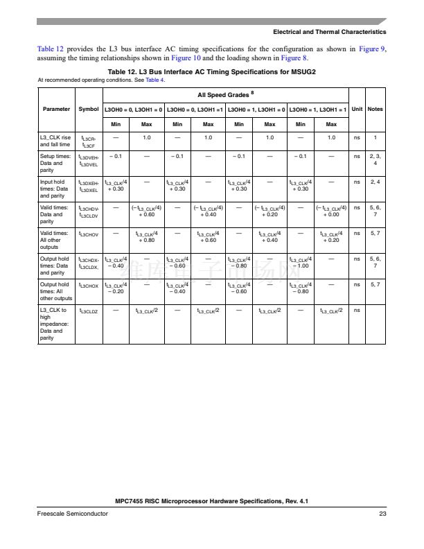
5.2.4.1 L3 Bus AC Specifications for DDR MSUG2 SRAMs
When using DDR MSUG2 SRAMs at the L3 interface, the parts should be connected as shown in
Figure 9.
Outputs from the MPC7455 are actually launched on the edges of an internal clock phase-aligned to SYSCLK
(adjusted for core and L3 frequency divisors). L3_CLK0 and L3_CLK1 are this internal clock output with 90掳 phase
delay, so outputs are shown synchronous to L3_CLK0 and L3_CLK1. Output valid times are typically negative
when referenced to L3_CLKn because the data is launched one-quarter period before L3_CLKn to provide adequate
setup time at the SRAM after the delay-matched address, control, data, and L3_CLKn signals have propagated
across the printed-wiring board.
Inputs to the MPC7455 are source-synchronous with the CQ clock generated by the DDR MSUG2 SRAMs. These
CQ clocks are received on the L3_ECHO_CLKn inputs of the MPC7455. An internal circuit delays the incoming
L3_ECHO_CLKn signal such that it is positioned within the valid data window at the internal receiving latches. This
delayed clock is used to capture the data into these latches which comprise the receive FIFO. This clock is
asynchronous to all other processor clocks. This latched data is subsequently read out of the FIFO synchronously to
the processor clock. The time between writing and reading the data is set by the using the sample point settings
defined in the L3CR register.
MPC7455 RISC Microprocessor Hardware Specifications, Rev. 4.1
22
Freescale Semiconductor


 1
1
 2
2
 3
3
 4
4
 5
5
 6
6
 7
7
 8
8
 9
9
 10
10
 11
11
 12
12
 13
13
 14
14
 15
15
 16
16
 17
17
 18
18
 19
19
 20
20
 21
21
 22
22
 23
23
 24
24
 25
25
 26
26
 27
27
 28
28
 29
29
 30
30
 31
31
 32
32
 33
33
 34
34
 35
35
 36
36
 37
37
 38
38
 39
39
 40
40
 41
41
 42
42
 43
43
 44
44
 45
45
 46
46
 47
47
 48
48
 49
49
 50
50
 51
51
 52
52
 53
53
 54
54
 55
55
 56
56
 57
57
 58
58
 59
59
 60
60
 61
61
 62
62
 63
63
 64
64
