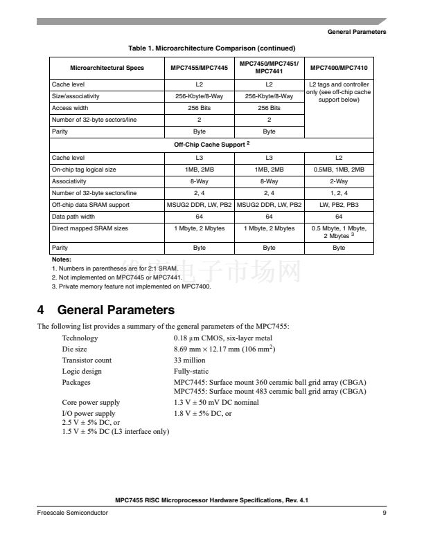
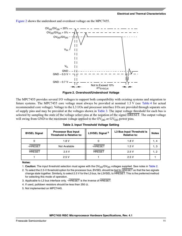
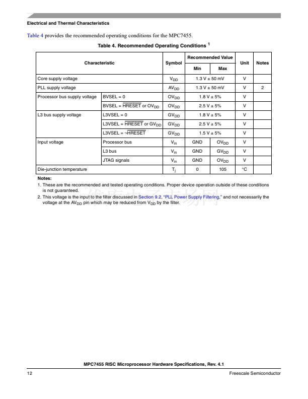
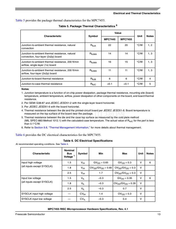
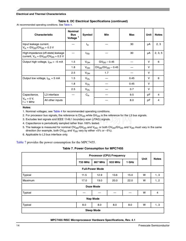
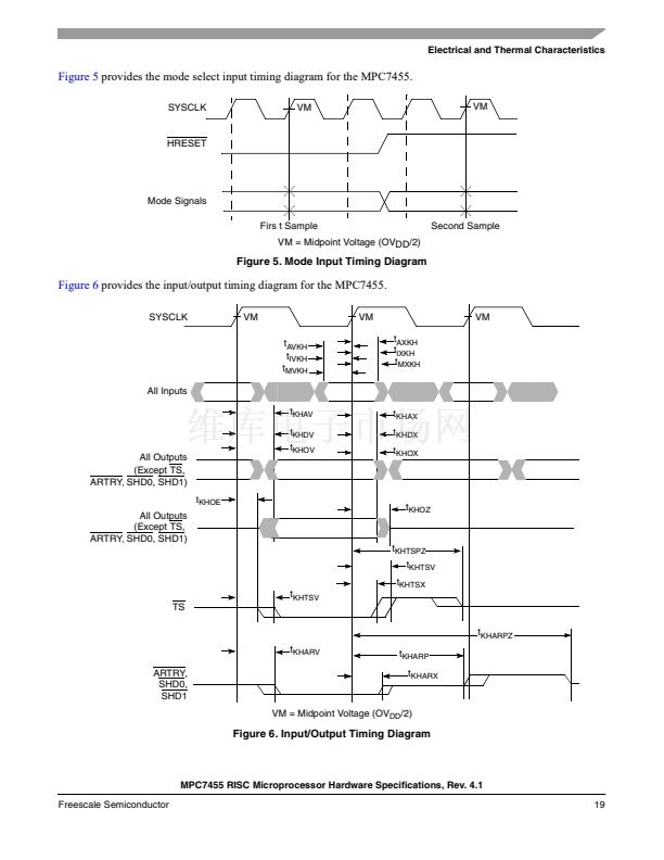
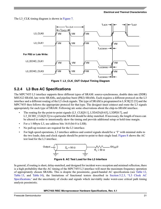
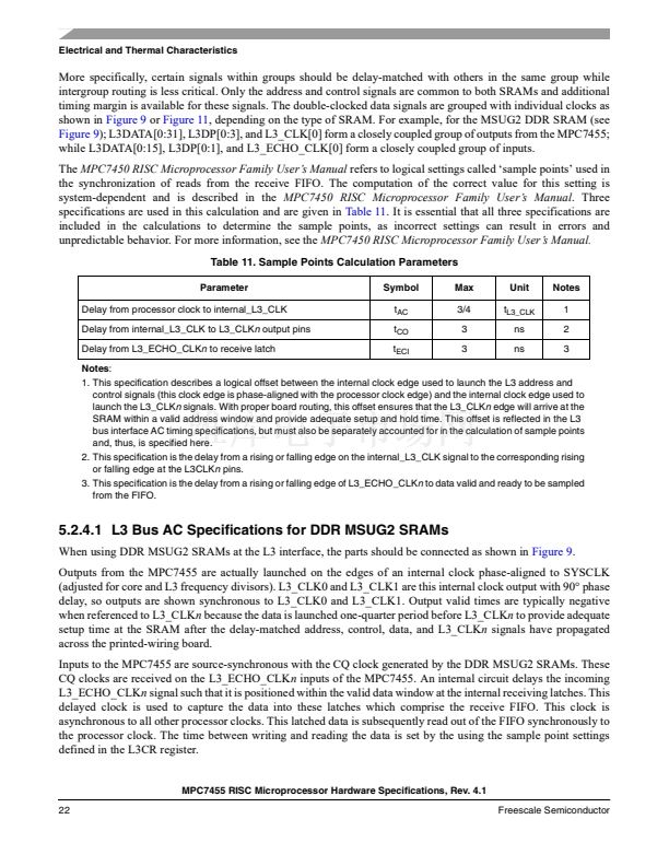
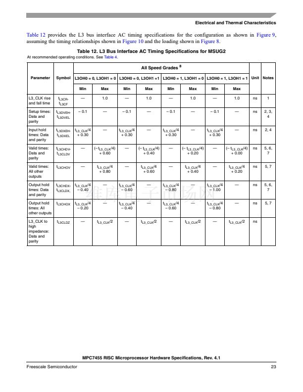
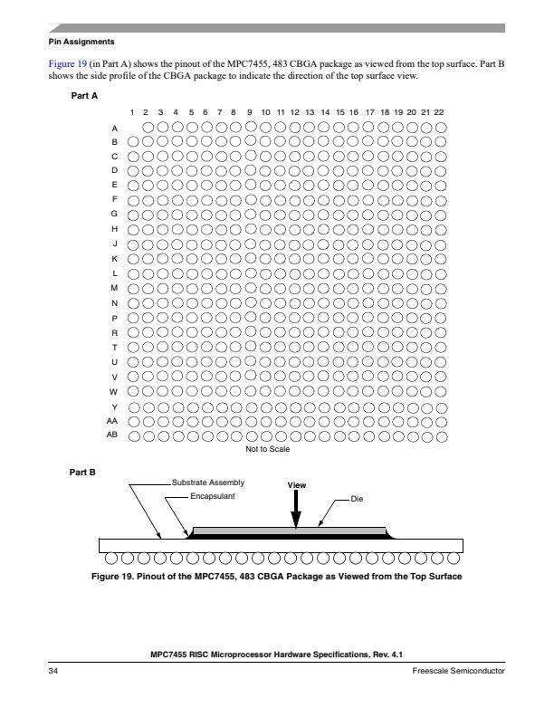
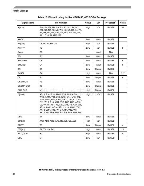
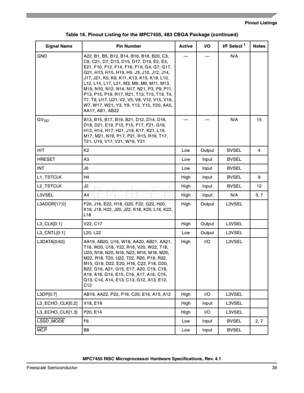
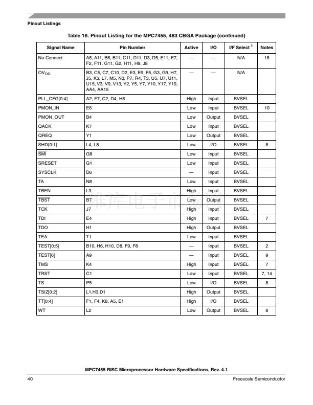
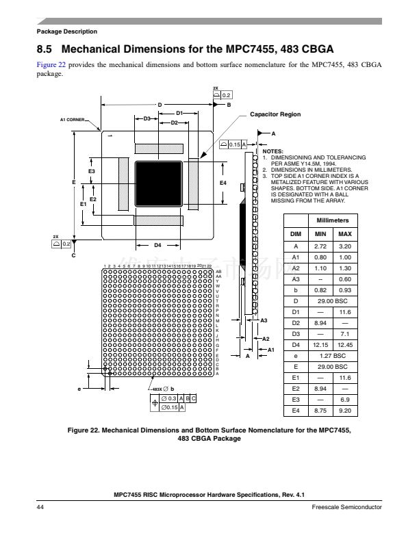
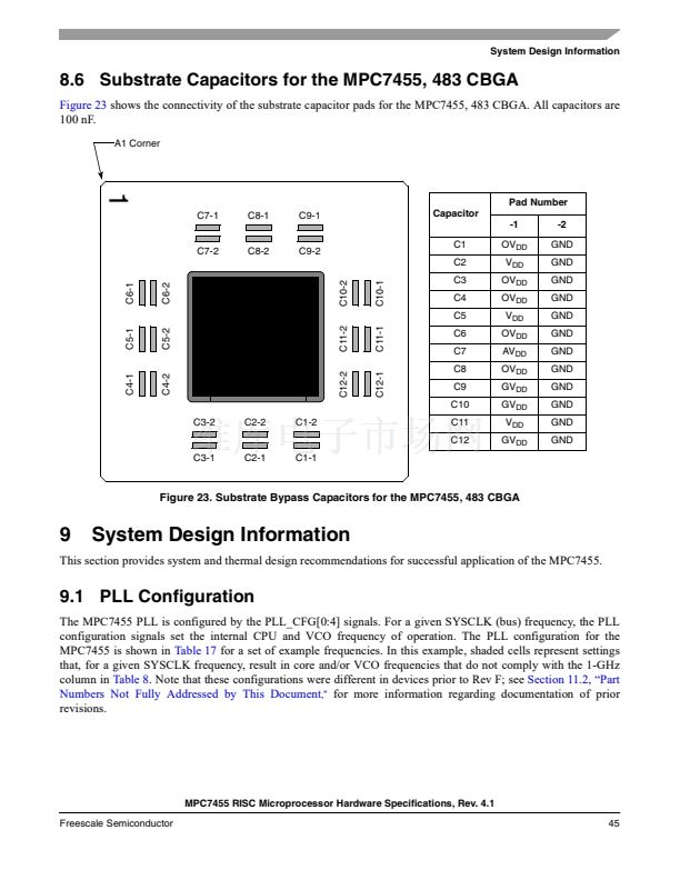
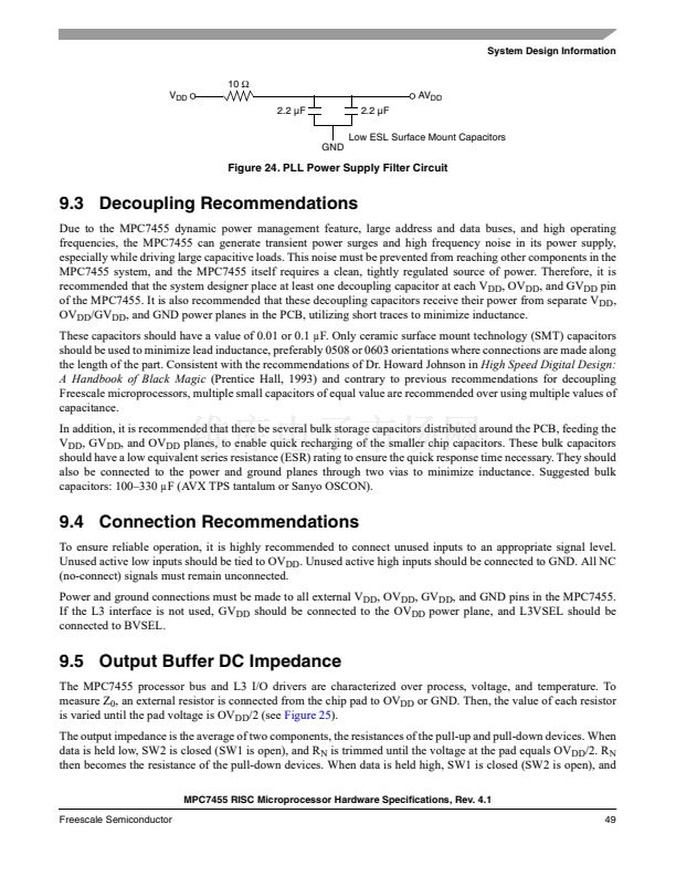
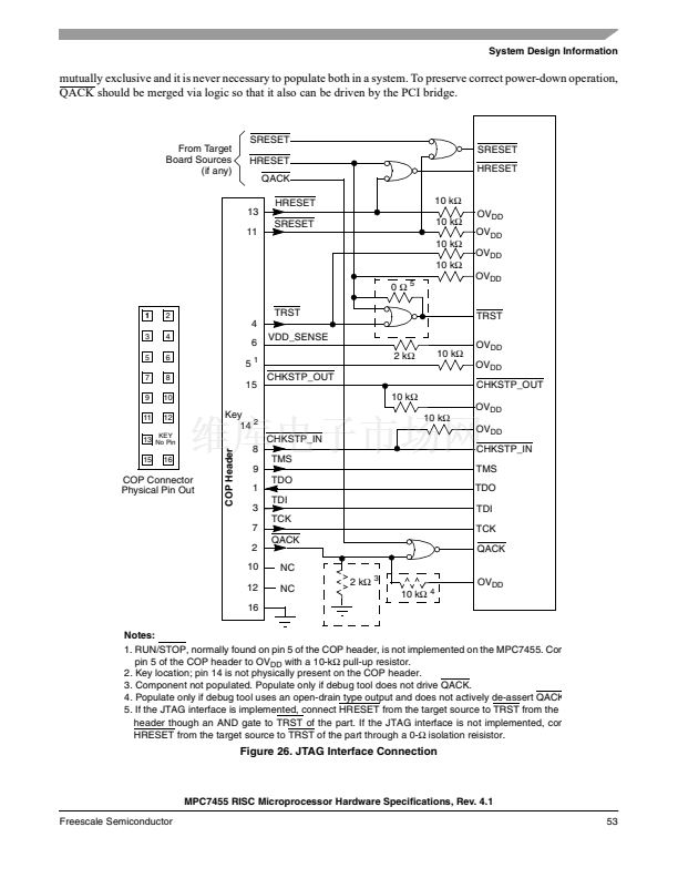
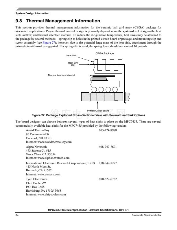
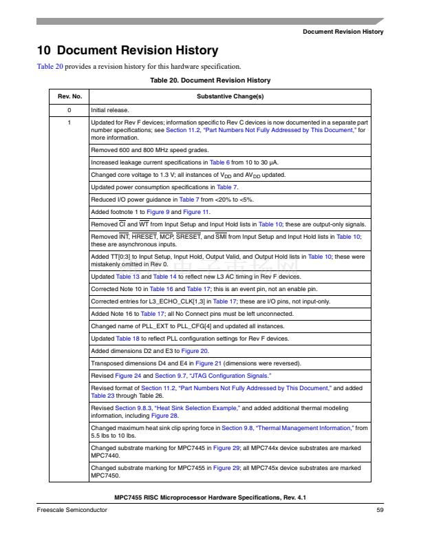
System Design Information
8.6 Substrate Capacitors for the MPC7455, 483 CBGA
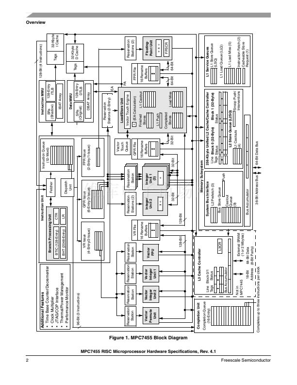
Figure 23
shows the connectivity of the substrate capacitor pads for the MPC7455, 483 CBGA. All capacitors are
100 nF.
A1 Corner
C10-2
C10-1
C6-1
C6-2
C11-2
C11-1
C5-1
C5-2
C12-2
C12-1
C4-1
C4-2
1
C7-1
C8-1
C9-1
Capacitor
C7-2
C8-2
C9-2
C1
C2
C3
C4
C5
C6
C7
C8
C9
C10
C3-2
C2-2
C1-2
C11
C12
C3-1
C2-1
C1-1
Pad Number
-1
OV
DD
V
DD
OV
DD
OV
DD
V
DD
OV
DD
AV
DD
OV
DD
GV
DD
GV
DD
V
DD
GV
DD
-2
GND
GND
GND
GND
GND
GND
GND
GND
GND
GND
GND
GND
Figure 23. Substrate Bypass Capacitors for the MPC7455, 483 CBGA
9
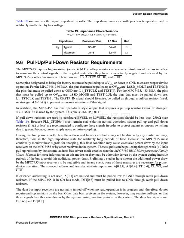
System Design Information
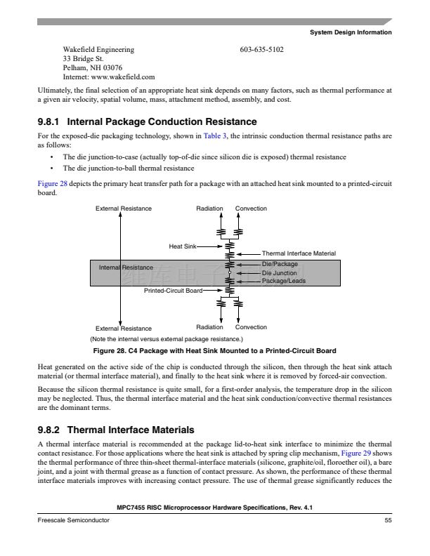
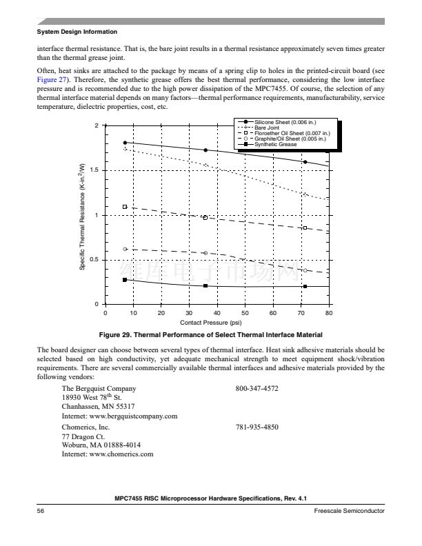
This section provides system and thermal design recommendations for successful application of the MPC7455.
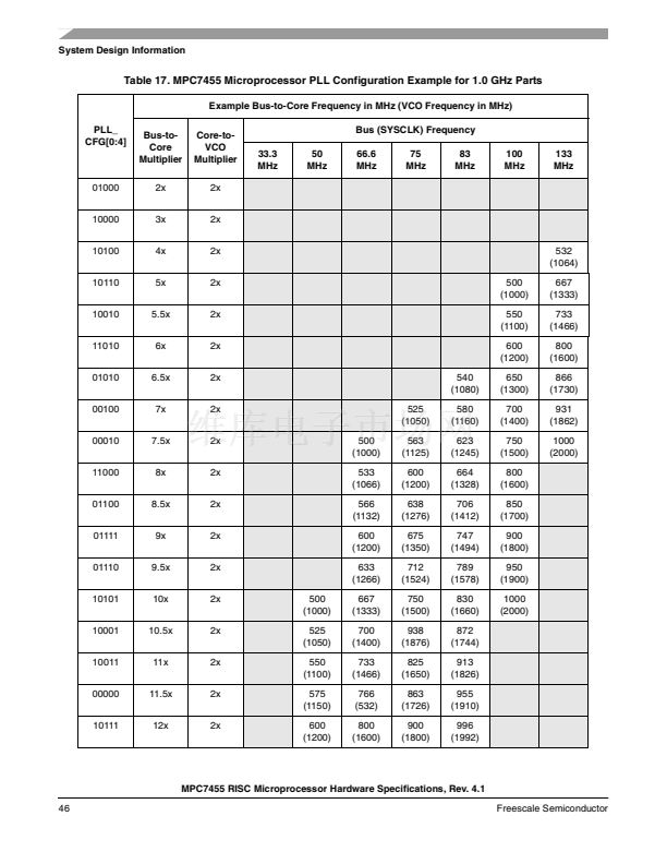
9.1 PLL Configuration
The MPC7455 PLL is configured by the PLL_CFG[0:4] signals. For a given SYSCLK (bus) frequency, the PLL
configuration signals set the internal CPU and VCO frequency of operation. The PLL configuration for the
MPC7455 is shown in
Table 17
for a set of example frequencies. In this example, shaded cells represent settings
that, for a given SYSCLK frequency, result in core and/or VCO frequencies that do not comply with the 1-GHz
column in
Table 8.
Note that these configurations were different in devices prior to Rev F; see
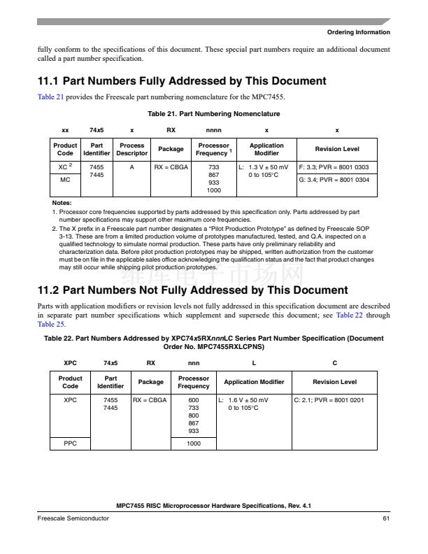
Section 11.2, 鈥淧art
Numbers Not Fully Addressed by This Document
,鈥?/div>
for more information regarding documentation of prior
revisions.
MPC7455 RISC Microprocessor Hardware Specifications, Rev. 4.1
Freescale Semiconductor
45


 1
1
 2
2
 3
3
 4
4
 5
5
 6
6
 7
7
 8
8
 9
9
 10
10
 11
11
 12
12
 13
13
 14
14
 15
15
 16
16
 17
17
 18
18
 19
19
 20
20
 21
21
 22
22
 23
23
 24
24
 25
25
 26
26
 27
27
 28
28
 29
29
 30
30
 31
31
 32
32
 33
33
 34
34
 35
35
 36
36
 37
37
 38
38
 39
39
 40
40
 41
41
 42
42
 43
43
 44
44
 45
45
 46
46
 47
47
 48
48
 49
49
 50
50
 51
51
 52
52
 53
53
 54
54
 55
55
 56
56
 57
57
 58
58
 59
59
 60
60
 61
61
 62
62
 63
63
 64
64
