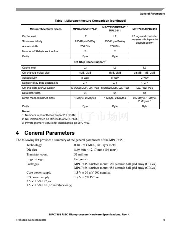
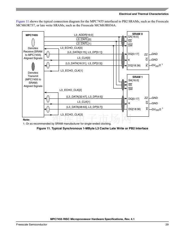
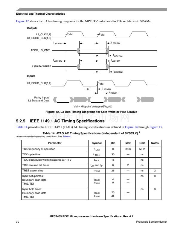
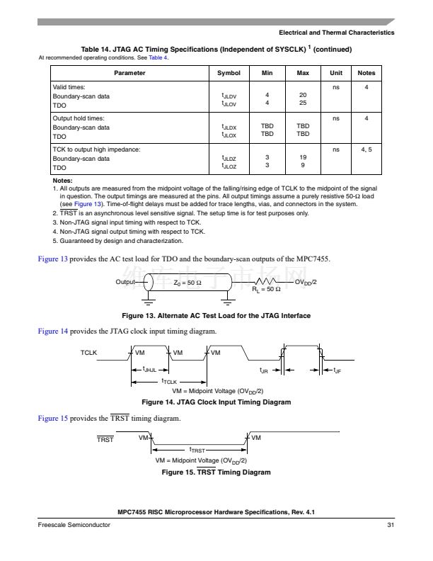
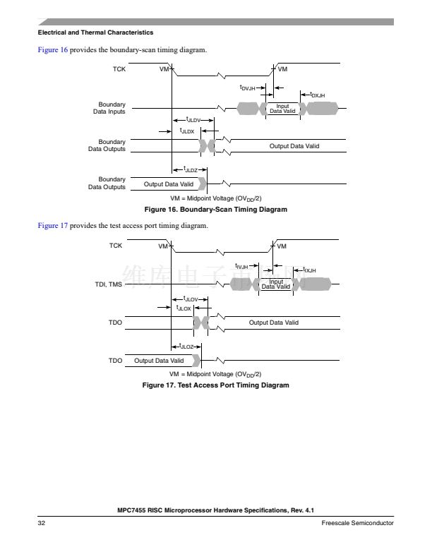
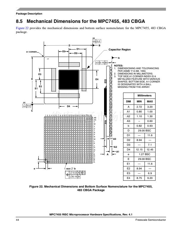
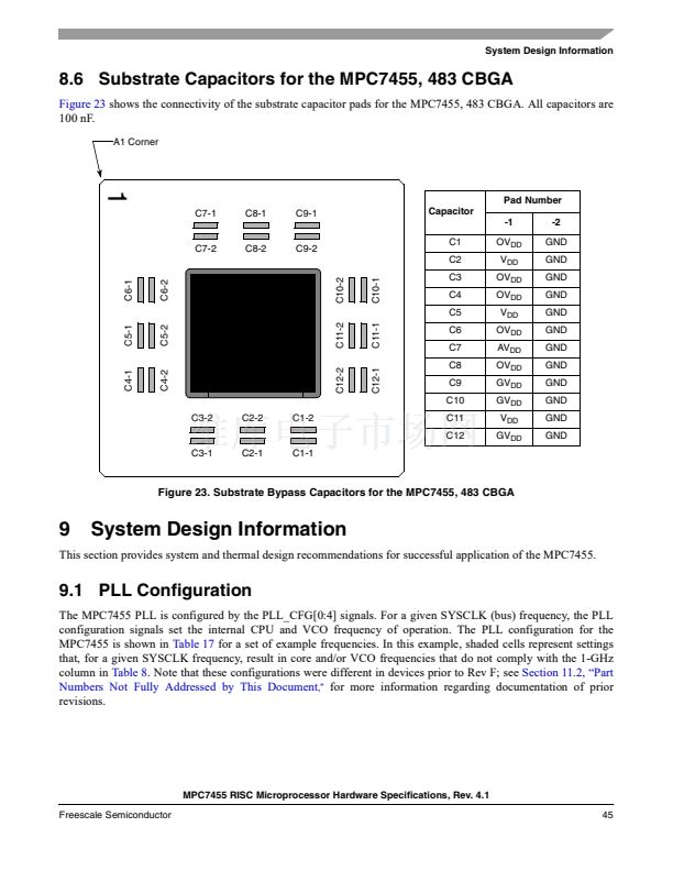
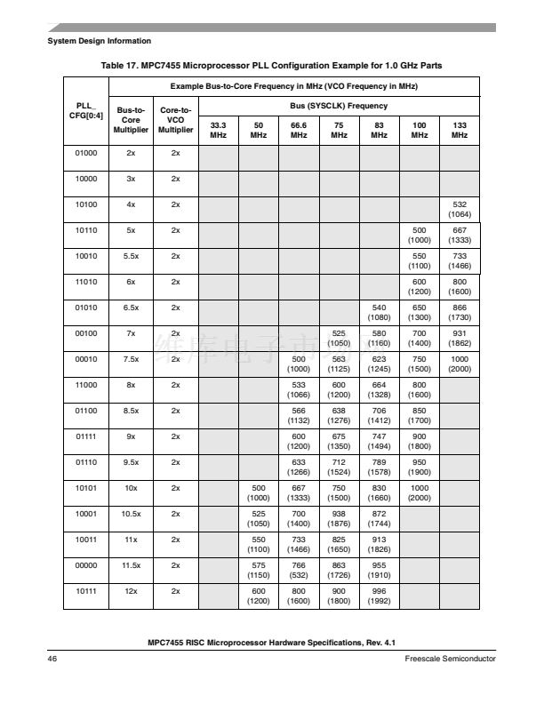
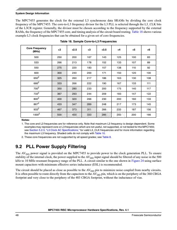
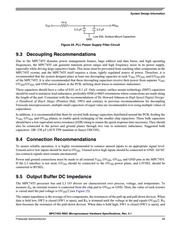
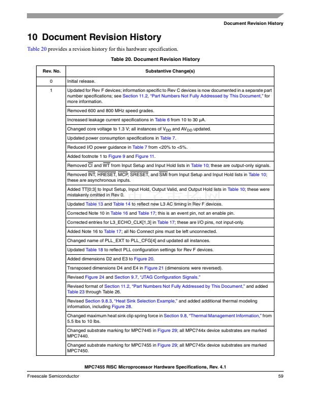
鈩?/div>
V
DD
2.2 碌F
2.2 碌F
Low ESL Surface Mount Capacitors
GND
AV
DD
Figure 24. PLL Power Supply Filter Circuit
9.3 Decoupling Recommendations
Due to the MPC7455 dynamic power management feature, large address and data buses, and high operating
frequencies, the MPC7455 can generate transient power surges and high frequency noise in its power supply,
especially while driving large capacitive loads. This noise must be prevented from reaching other components in the
MPC7455 system, and the MPC7455 itself requires a clean, tightly regulated source of power. Therefore, it is
recommended that the system designer place at least one decoupling capacitor at each V
DD
, OV
DD
, and GV
DD
pin
of the MPC7455. It is also recommended that these decoupling capacitors receive their power from separate V
DD
,
OV
DD
/GV
DD
, and GND power planes in the PCB, utilizing short traces to minimize inductance.
These capacitors should have a value of 0.01 or 0.1 碌F. Only ceramic surface mount technology (SMT) capacitors
should be used to minimize lead inductance, preferably 0508 or 0603 orientations where connections are made along
the length of the part. Consistent with the recommendations of Dr. Howard Johnson in
High Speed Digital Design:
A Handbook of Black Magic
(Prentice Hall, 1993) and contrary to previous recommendations for decoupling
Freescale microprocessors, multiple small capacitors of equal value are recommended over using multiple values of
capacitance.
In addition, it is recommended that there be several bulk storage capacitors distributed around the PCB, feeding the
V
DD
, GV
DD
, and OV
DD
planes, to enable quick recharging of the smaller chip capacitors. These bulk capacitors
should have a low equivalent series resistance (ESR) rating to ensure the quick response time necessary. They should
also be connected to the power and ground planes through two vias to minimize inductance. Suggested bulk
capacitors: 100鈥?30 碌F (AVX TPS tantalum or Sanyo OSCON).
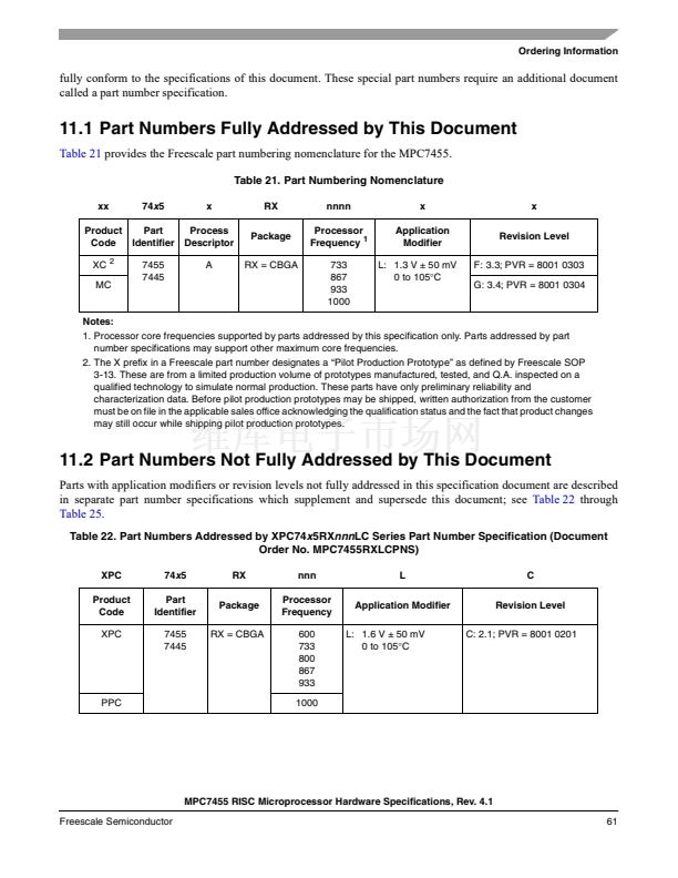
9.4 Connection Recommendations
To ensure reliable operation, it is highly recommended to connect unused inputs to an appropriate signal level.
Unused active low inputs should be tied to OV
DD
. Unused active high inputs should be connected to GND. All NC
(no-connect) signals must remain unconnected.
Power and ground connections must be made to all external V
DD
, OV
DD
, GV
DD
, and GND pins in the MPC7455.
If the L3 interface is not used, GV
DD
should be connected to the OV
DD
power plane, and L3VSEL should be
connected to BVSEL.
9.5 Output Buffer DC Impedance
The MPC7455 processor bus and L3 I/O drivers are characterized over process, voltage, and temperature. To
measure Z
0
, an external resistor is connected from the chip pad to OV
DD
or GND. Then, the value of each resistor
is varied until the pad voltage is OV
DD
/2 (see
Figure 25).
The output impedance is the average of two components, the resistances of the pull-up and pull-down devices. When
data is held low, SW2 is closed (SW1 is open), and R
N
is trimmed until the voltage at the pad equals OV
DD
/2. R
N
then becomes the resistance of the pull-down devices. When data is held high, SW1 is closed (SW2 is open), and
MPC7455 RISC Microprocessor Hardware Specifications, Rev. 4.1
Freescale Semiconductor
49


 1
1
 2
2
 3
3
 4
4
 5
5
 6
6
 7
7
 8
8
 9
9
 10
10
 11
11
 12
12
 13
13
 14
14
 15
15
 16
16
 17
17
 18
18
 19
19
 20
20
 21
21
 22
22
 23
23
 24
24
 25
25
 26
26
 27
27
 28
28
 29
29
 30
30
 31
31
 32
32
 33
33
 34
34
 35
35
 36
36
 37
37
 38
38
 39
39
 40
40
 41
41
 42
42
 43
43
 44
44
 45
45
 46
46
 47
47
 48
48
 49
49
 50
50
 51
51
 52
52
 53
53
 54
54
 55
55
 56
56
 57
57
 58
58
 59
59
 60
60
 61
61
 62
62
 63
63
 64
64
