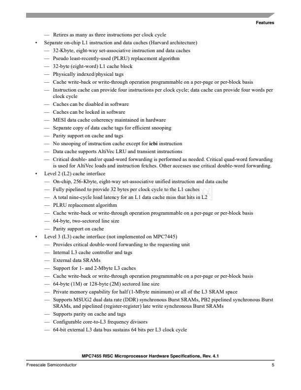
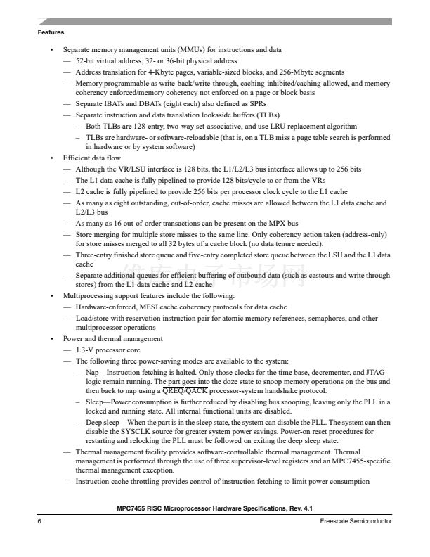
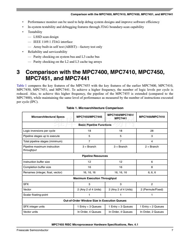
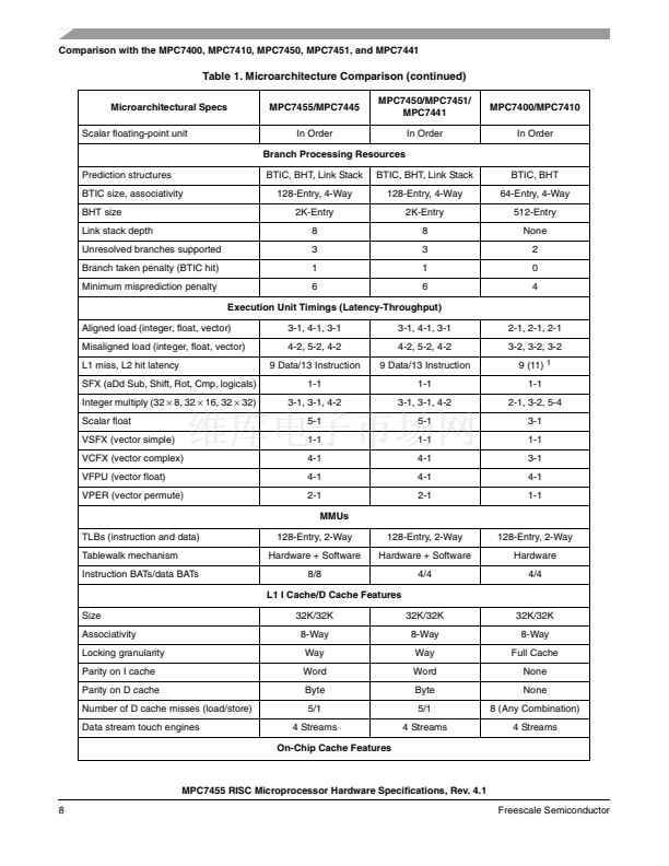
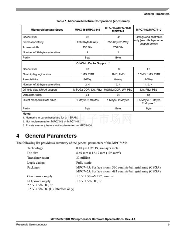
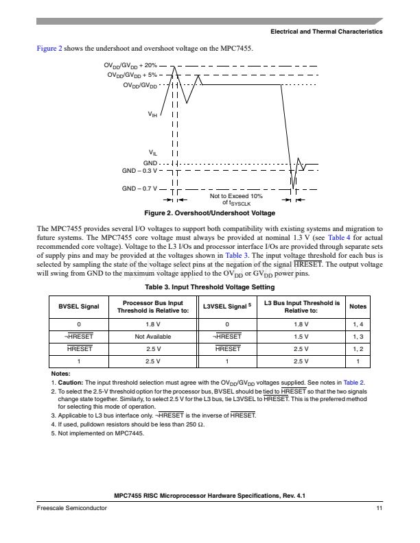
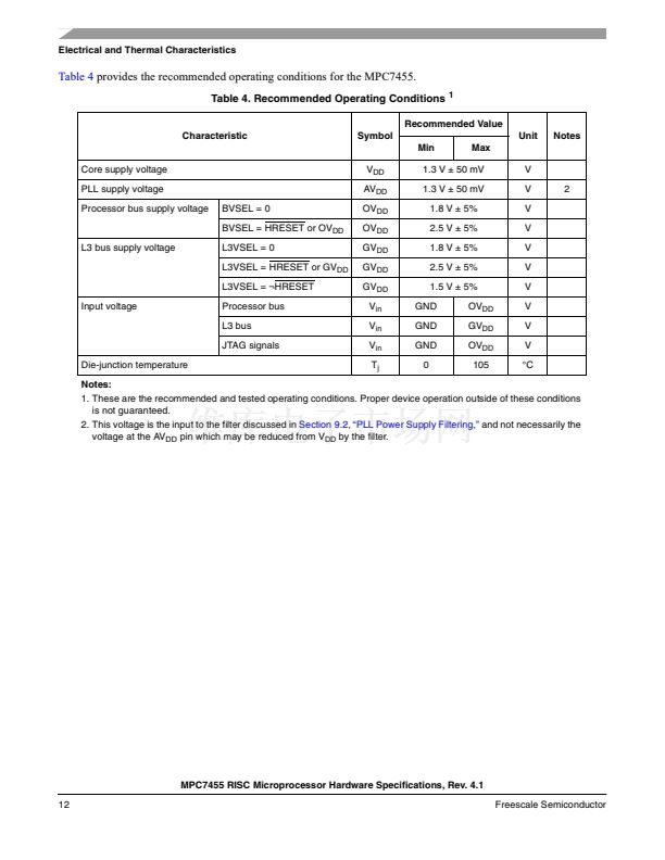
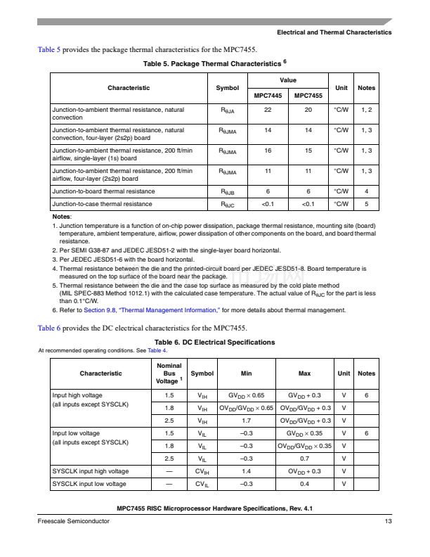
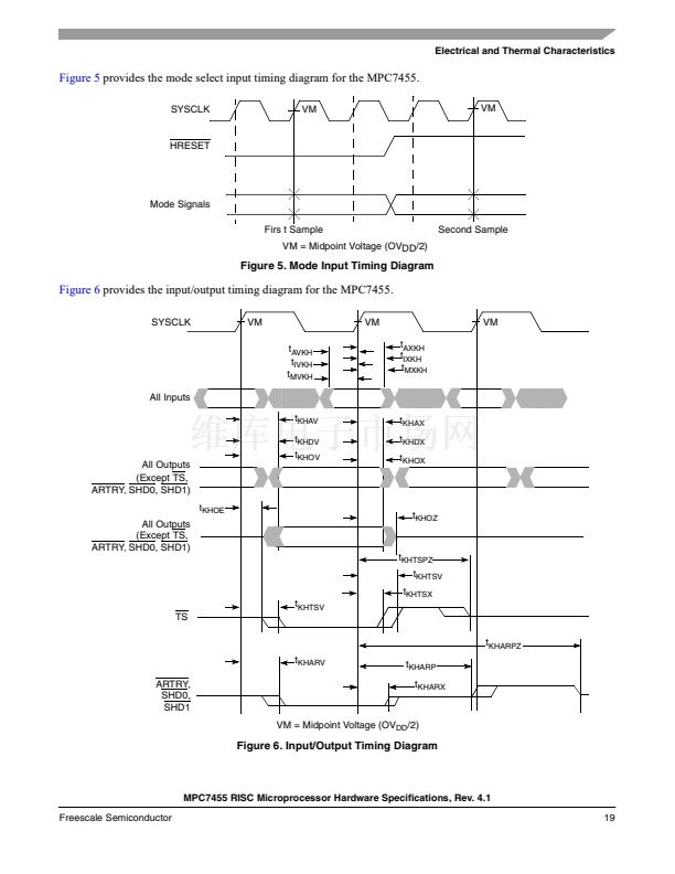
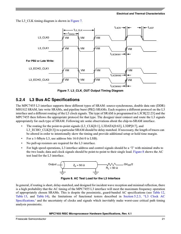
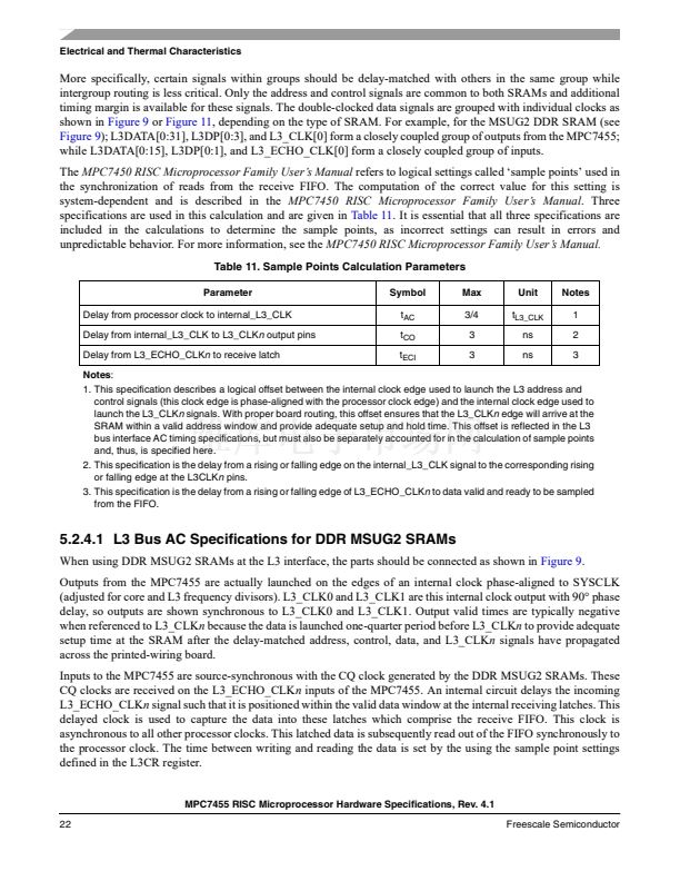
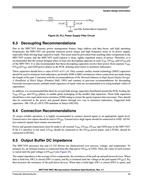
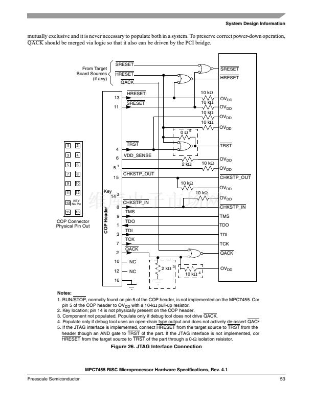
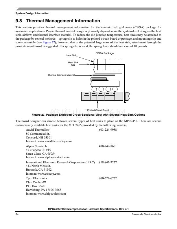
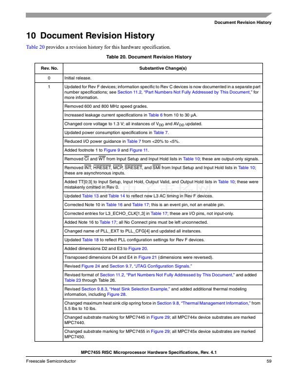
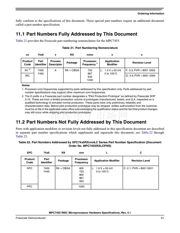
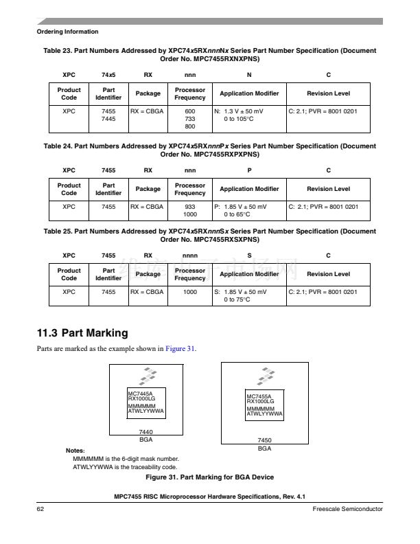
鈩?/div>
9.6 Pull-Up/Pull-Down Resistor Requirements
The MPC7455 requires high-resistive (weak: 4.7-k鈩? pull-up resistors on several control pins of the bus interface
to maintain the control signals in the negated state after they have been actively negated and released by the
MPC7455 or other bus masters. These pins are: TS, ARTRY, SHDO, and SHD1.
Some pins designated as being for factory test must be pulled up to OV
DD
or down to GND to ensure proper device
operation. For the MPC7445, 360 BGA, the pins that must be pulled up to OV
DD
are: LSSD_MODE and TEST[0:3];
the pins that must be pulled down to GND are: L1_TSTCLK and TEST[4]. For the MPC7455, 483 BGA, the pins
that must be pulled up to OV
DD
are: LSSD_MODE and TEST[0:5]; the pins that must be pulled down are:
L1_TSTCLK and TEST[6]. The CKSTP_IN signal should likewise, be pulled up through a pull-up resistor (weak
or stronger: 4.7鈥? k鈩? to prevent erroneous assertions of this signal
In addition, the MPC7455 has one open-drain style output that requires a pull-up resistor (weak or stronger:
4.7鈥? k鈩? if it is used by the system. This pin is CKSTP_OUT.
If pull-down resistors are used to configure BVSEL or L3VSEL, the resistors should be less than 250
鈩?/div>
(see
Table 16).
Because PLL_CFG[0:4] must remain stable during normal operation, strong pull-up and pull-down
resistors (1 k鈩?or less) are recommended to configure these signals in order to protect against erroneous switching
due to ground bounce, power supply noise or noise coupling.
During inactive periods on the bus, the address and transfer attributes may not be driven by any master and may,
therefore, float in the high-impedance state for relatively long periods of time. Because the MPC7455 must
continually monitor these signals for snooping, this float condition may cause excessive power draw by the input
receivers on the MPC7455 or by other receivers in the system. These signals can be pulled up through weak (10-k鈩?
pull-up resistors by the system, address bus driven mode enabled (see the
MPC7450 RISC Microporcessor Family
Users鈥?Manual
for more information on this mode), or they may be otherwise driven by the system during inactive
periods of the bus to avoid this additional power draw. Preliminary studies have shown the additional power draw
by the MPC7455 input receivers to be negligible and, in any event, none of these measures are necessary for proper
device operation. The snooped address and transfer attribute inputs are: A[0:35], AP[0:4], TT[0:4], CI, WT, and
GBL.
If extended addressing is not used, A[0:3] are unused and must be pulled low to GND through weak pull-down
resistors. If the MPC7455 is in 60x bus mode, DTI[0:3] must be pulled low to GND through weak pull-down
resistors.
The data bus input receivers are normally turned off when no read operation is in progress and, therefore, do not
require pull-up resistors on the bus. Other data bus receivers in the system, however, may require pull-ups, or that
those signals be otherwise driven by the system during inactive periods by the system. The data bus signals are:
D[0:63] and DP[0:7].
MPC7455 RISC Microprocessor Hardware Specifications, Rev. 4.1
Freescale Semiconductor
51


 1
1
 2
2
 3
3
 4
4
 5
5
 6
6
 7
7
 8
8
 9
9
 10
10
 11
11
 12
12
 13
13
 14
14
 15
15
 16
16
 17
17
 18
18
 19
19
 20
20
 21
21
 22
22
 23
23
 24
24
 25
25
 26
26
 27
27
 28
28
 29
29
 30
30
 31
31
 32
32
 33
33
 34
34
 35
35
 36
36
 37
37
 38
38
 39
39
 40
40
 41
41
 42
42
 43
43
 44
44
 45
45
 46
46
 47
47
 48
48
 49
49
 50
50
 51
51
 52
52
 53
53
 54
54
 55
55
 56
56
 57
57
 58
58
 59
59
 60
60
 61
61
 62
62
 63
63
 64
64
