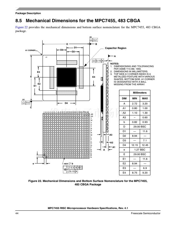
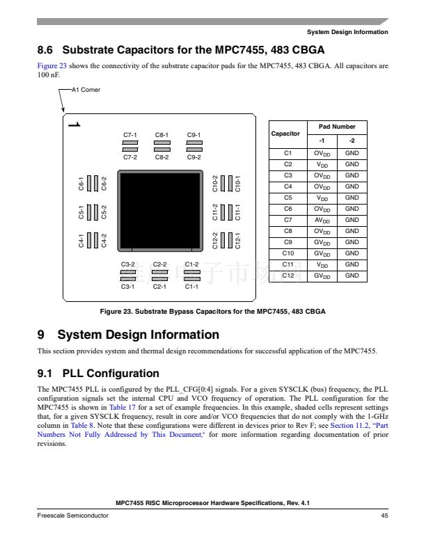
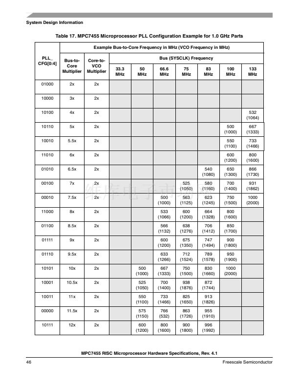
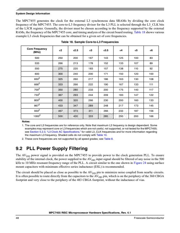
鈥?/div>
Separate memory management units (MMUs) for instructions and data
鈥?52-bit virtual address; 32- or 36-bit physical address
鈥?Address translation for 4-Kbyte pages, variable-sized blocks, and 256-Mbyte segments
鈥?Memory programmable as write-back/write-through, caching-inhibited/caching-allowed, and memory
coherency enforced/memory coherency not enforced on a page or block basis
鈥?Separate IBATs and DBATs (eight each) also defined as SPRs
鈥?Separate instruction and data translation lookaside buffers (TLBs)
鈥?Both TLBs are 128-entry, two-way set-associative, and use LRU replacement algorithm
鈥?TLBs are hardware- or software-reloadable (that is, on a TLB miss a page table search is performed
in hardware or by system software)
Efficient data flow
鈥?Although the VR/LSU interface is 128 bits, the L1/L2/L3 bus interface allows up to 256 bits
鈥?The L1 data cache is fully pipelined to provide 128 bits/cycle to or from the VRs
鈥?L2 cache is fully pipelined to provide 256 bits per processor clock cycle to the L1 cache
鈥?As many as eight outstanding, out-of-order, cache misses are allowed between the L1 data cache and
L2/L3 bus
鈥?As many as 16 out-of-order transactions can be present on the MPX bus
鈥?Store merging for multiple store misses to the same line. Only coherency action taken (address-only)
for store misses merged to all 32 bytes of a cache block (no data tenure needed).
鈥?Three-entry finished store queue and five-entry completed store queue between the LSU and the L1 data
cache
鈥?Separate additional queues for efficient buffering of outbound data (such as castouts and write through
stores) from the L1 data cache and L2 cache
Multiprocessing support features include the following:
鈥?Hardware-enforced, MESI cache coherency protocols for data cache
鈥?Load/store with reservation instruction pair for atomic memory references, semaphores, and other
multiprocessor operations
Power and thermal management
鈥?1.3-V processor core
鈥?The following three power-saving modes are available to the system:
鈥?Nap鈥擨nstruction fetching is halted. Only those clocks for the time base, decrementer, and JTAG
logic remain running. The part goes into the doze state to snoop memory operations on the bus and
then back to nap using a QREQ/QACK processor-system handshake protocol.
鈥?Sleep鈥擯ower consumption is further reduced by disabling bus snooping, leaving only the PLL in a
locked and running state. All internal functional units are disabled.
鈥?Deep sleep鈥擶hen the part is in the sleep state, the system can disable the PLL. The system can then
disable the SYSCLK source for greater system power savings. Power-on reset procedures for
restarting and relocking the PLL must be followed on exiting the deep sleep state.
鈥?Thermal management facility provides software-controllable thermal management. Thermal
management is performed through the use of three supervisor-level registers and an MPC7455-specific
thermal management exception.
鈥?Instruction cache throttling provides control of instruction fetching to limit power consumption
MPC7455 RISC Microprocessor Hardware Specifications, Rev. 4.1
6
Freescale Semiconductor


 1
1
 2
2
 3
3
 4
4
 5
5
 6
6
 7
7
 8
8
 9
9
 10
10
 11
11
 12
12
 13
13
 14
14
 15
15
 16
16
 17
17
 18
18
 19
19
 20
20
 21
21
 22
22
 23
23
 24
24
 25
25
 26
26
 27
27
 28
28
 29
29
 30
30
 31
31
 32
32
 33
33
 34
34
 35
35
 36
36
 37
37
 38
38
 39
39
 40
40
 41
41
 42
42
 43
43
 44
44
 45
45
 46
46
 47
47
 48
48
 49
49
 50
50
 51
51
 52
52
 53
53
 54
54
 55
55
 56
56
 57
57
 58
58
 59
59
 60
60
 61
61
 62
62
 63
63
 64
64
