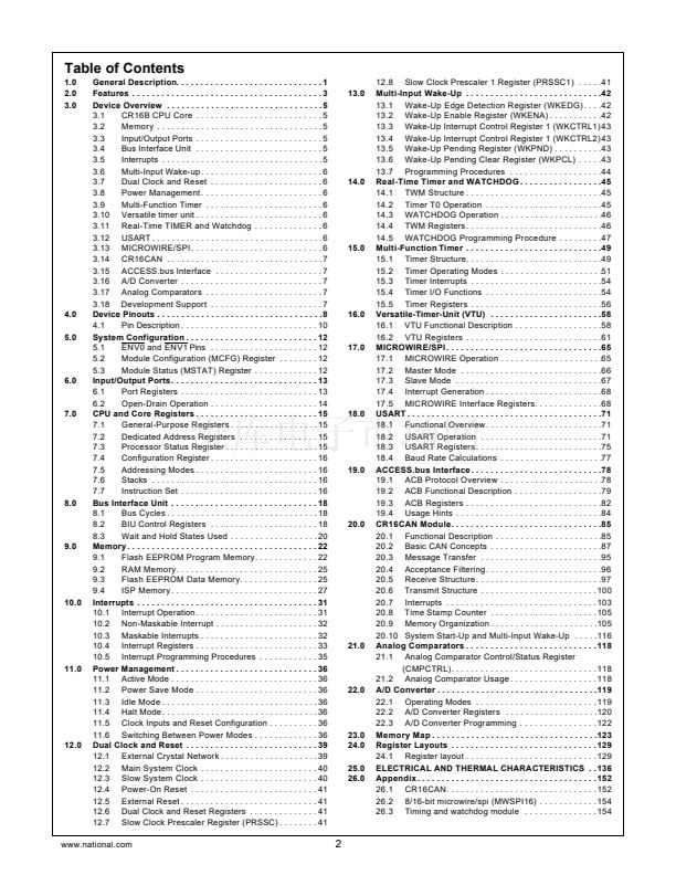
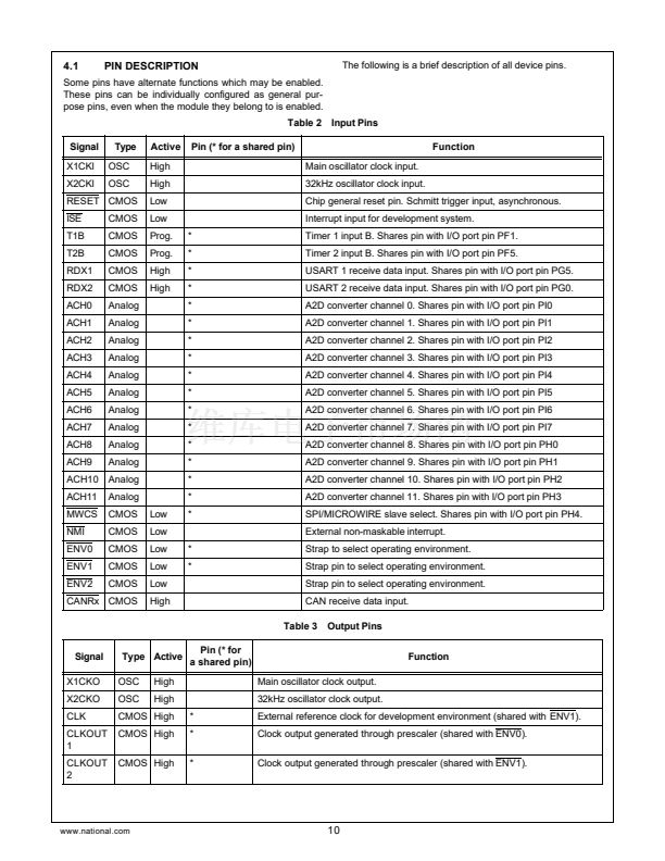
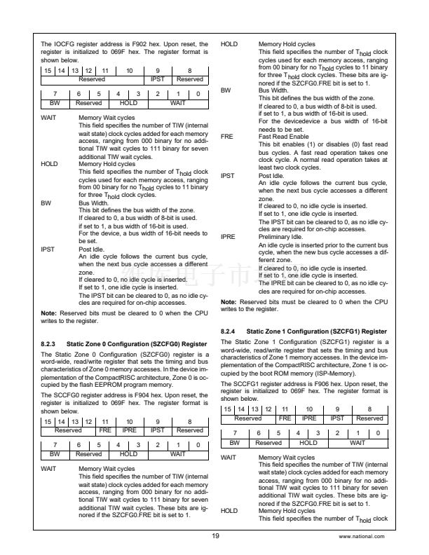
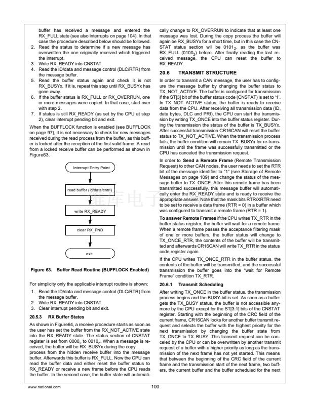
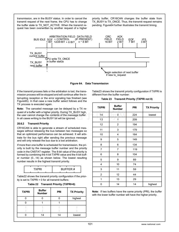
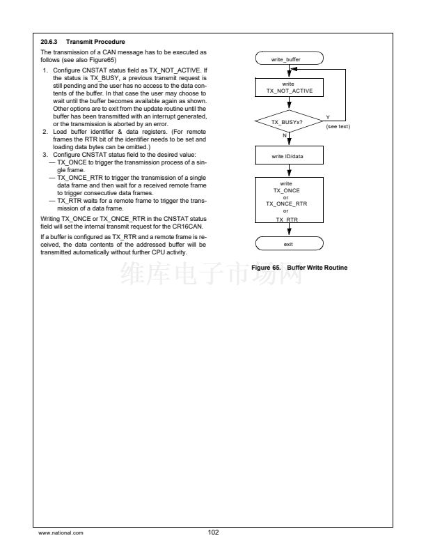
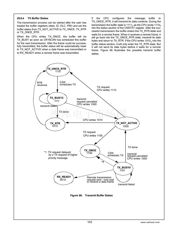
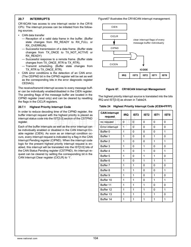
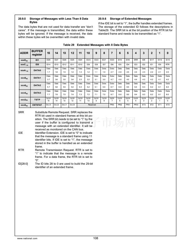
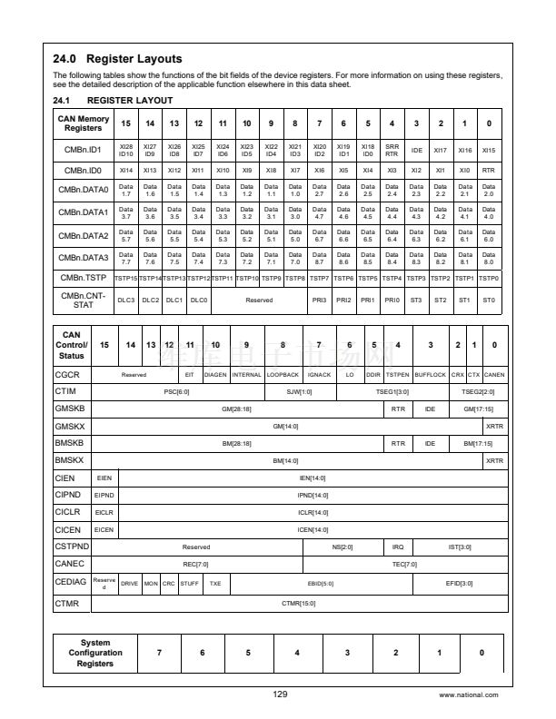
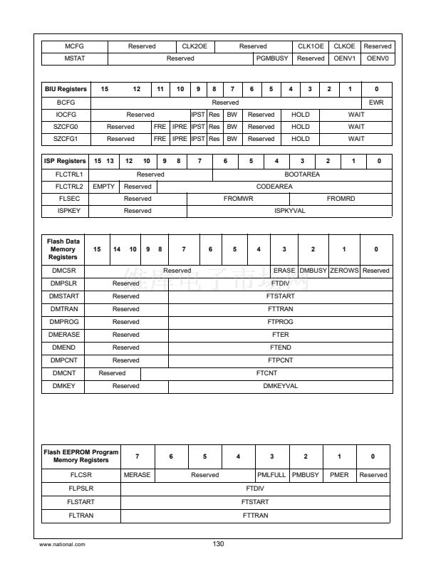
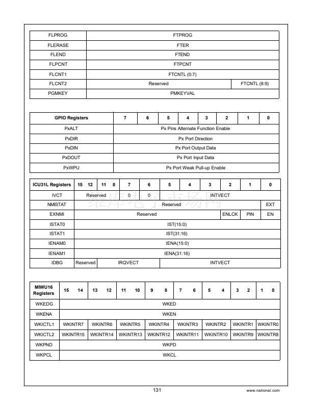
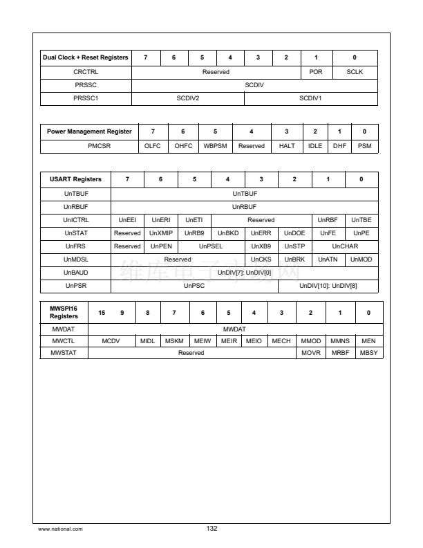
The IOCFG register address is F902 hex. Upon reset, the
register is initialized to 069F hex. The register format is
shown below.
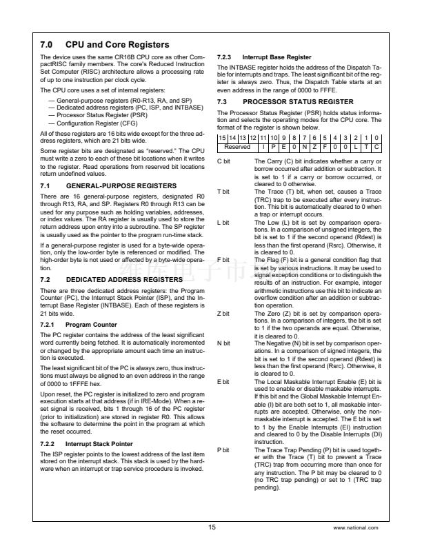
15
14
13
12
11
Reserved
10
9
IPST
2
8
Reserved
1
WAIT
0
HOLD
7
BW
WAIT
6
5
Reserved
4
3
HOLD
BW
HOLD
BW
IPST
Memory Wait cycles
This field specifies the number of TIW (internal
wait state) clock cycles added for each memory
access, ranging from 000 binary for no addi-
tional TIW wait cycles to 111 binary for seven
additional TIW wait cycles.
Memory Hold cycles
This field specifies the number of Thold clock
cycles used for each memory access, ranging
from 00 binary for no Thold cycles to 11 binary
for three Thold clock cycles.
Bus Width.
This bit defines the bus width of the zone.
If cleared to 0, a bus width of 8-bit is used.
if set to 1, a bus width of 16-bit is used.
For the device, a bus width of 16-bit needs to
be set.
Post Idle.
An idle cycle follows the current bus cycle,
when the next bus cycle accesses a different
zone.
If cleared to 0, no idle cycle is inserted.
If set to 1, one idle cycle is inserted.
The IPST bit can be cleared to 0, as no idle cy-
cles are required for on-chip accesses.
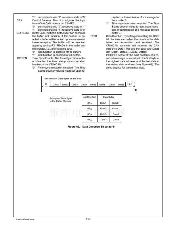
FRE
IPST
IPRE
Memory Hold cycles
This field specifies the number of Thold clock
cycles used for each memory access, ranging
from 00 binary for no Thold cycles to 11 binary
for three T hold clock cycles. These bits are ig-
nored if the SZCFG0.FRE bit is set to 1.
Bus Width.
This bit defines the bus width of the zone.
If cleared to 0, a bus width of 8-bit is used.
if set to 1, a bus width of 16-bit is used.
For the devicedevice a bus width of 16-bit
needs to be set.
Fast Read Enable
This bit enables (1) or disables (0) fast read
bus cycles. A fast read operation takes one
clock cycle. A normal read operation takes at
least two clock cycles.
Post Idle.
An idle cycle follows the current bus cycle,
when the next bus cycle accesses a different
zone.
If cleared to 0, no idle cycle is inserted.
If set to 1, one idle cycle is inserted.
The IPST bit can be cleared to 0, as no idle cy-
cles are required for on-chip accesses.
Preliminary Idle.
An idle cycle is inserted prior to the current bus
cycle, when the new bus cycle accesses a dif-
ferent zone.
If cleared to 0, no idle cycle is inserted.
If set to 1, one idle cycle is inserted.
The IPRE bit can be cleared to 0, as no idle cy-
cles are required for on-chip accesses.
Note:
Reserved bits must be cleared to 0 when the CPU
writes to the register.
Note:
Reserved bits must be cleared to 0 when the CPU
writes to the register.
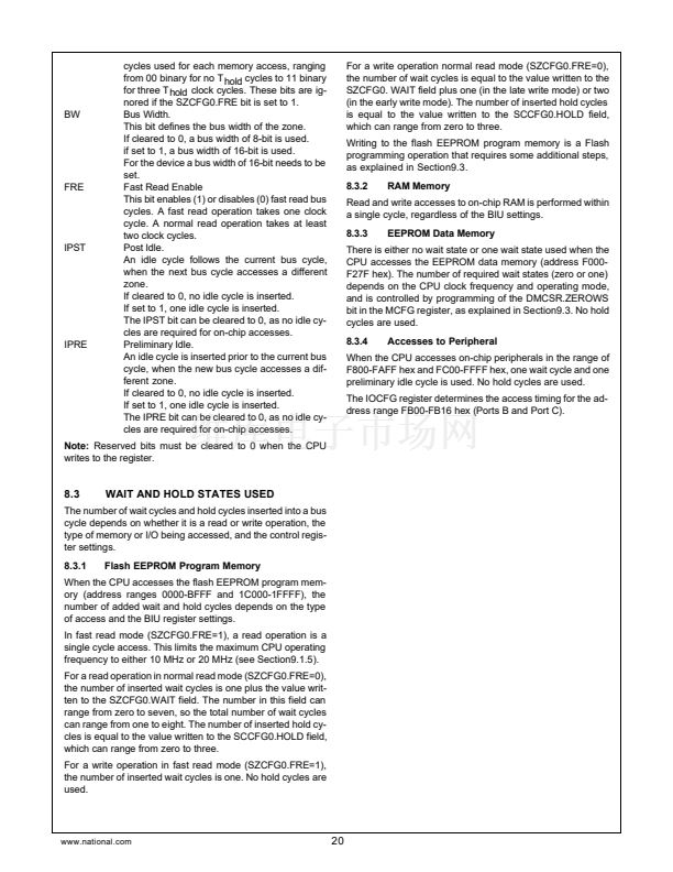
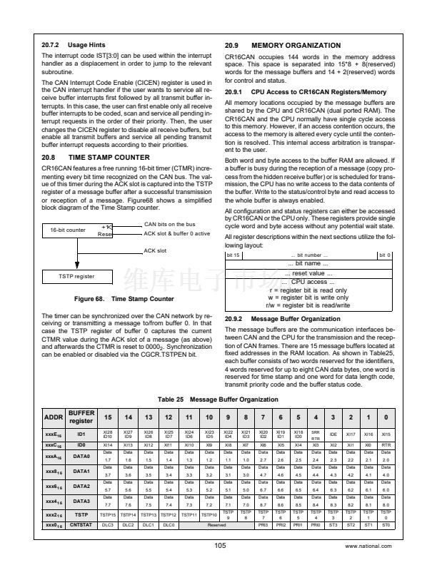
8.2.4
8.2.3
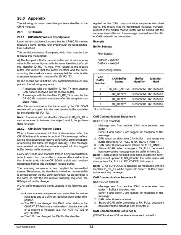
Static Zone 0 Configuration (SZCFG0) Register
Static Zone 1 Configuration (SZCFG1) Register
The Static Zone 0 Configuration (SZCFG0) register is a
word-wide, read/write register that sets the timing and bus
characteristics of Zone 0 memory accesses. In the device im-
plementation of the CompactRISC architecture, Zone 0 is oc-
cupied by the flash EEPROM program memory.
The SCCFG0 register address is F904 hex. Upon reset, the
register is initialized to 069F hex. The register format is
shown below.
15
14 13 12
Reserved
11
FRE
10
IPRE
4
3
HOLD
9
IPST
2
8
Reserved
1
WAIT
0
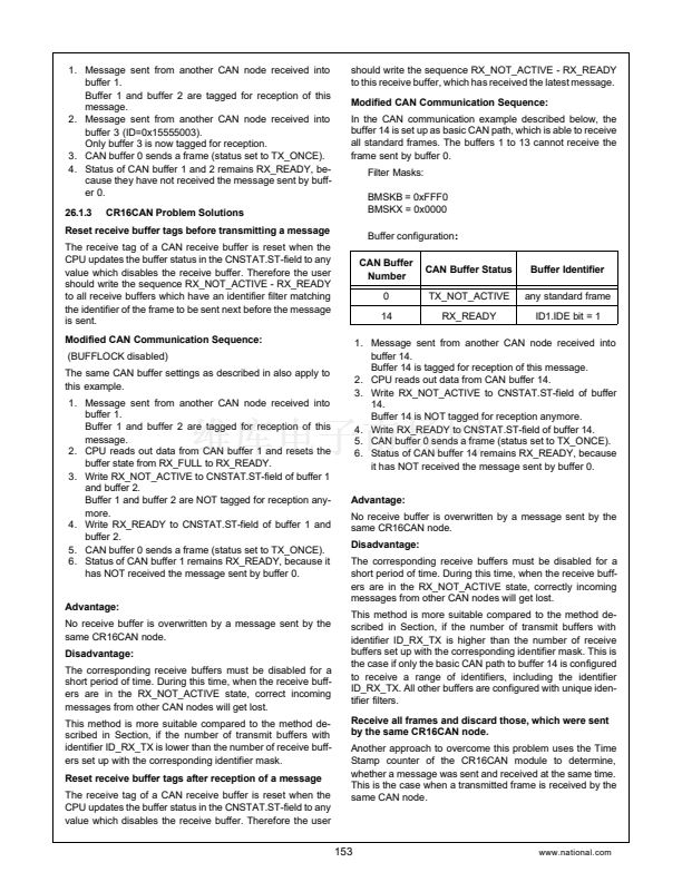
The Static Zone 1 Configuration (SZCFG1) register is a
word-wide, read/write register that sets the timing and bus
characteristics of Zone 1 memory accesses. In the device im-
plementation of the CompactRISC architecture, Zone 1 is oc-
cupied by the boot ROM memory (ISP-Memory).
The SCCFG1 register address is F906 hex. Upon reset, the
register is initialized to 069F hex. The register format is
shown below.
15
14 13 12
Reserved
11
FRE
10
IPRE
4
3
HOLD
9
IPST
2
8
Reserved
1
WAIT
0
7
BW
WAIT
6
5
Reserved
7
BW
WAIT
6
5
Reserved
Memory Wait cycles
This field specifies the number of TIW (internal
wait state) clock cycles added for each memory
access, ranging from 000 binary for no addi-
tional TIW wait cycles to 111 binary for seven
additional TIW wait cycles. These bits are ig-
nored if the SZCFG0.FRE bit is set to 1.
HOLD
Memory Wait cycles
This field specifies the number of TIW (internal
wait state) clock cycles added for each memory
access, ranging from 000 binary for no addi-
tional TIW wait cycles to 111 binary for seven
additional TIW wait cycles. These bits are ig-
nored if the SZCFG0.FRE bit is set to 1.
Memory Hold cycles
This field specifies the number of Thold clock
www.national.com
19


 1
1
 2
2
 3
3
 4
4
 5
5
 6
6
 7
7
 8
8
 9
9
 10
10
 11
11
 12
12
 13
13
 14
14
 15
15
 16
16
 17
17
 18
18
 19
19
 20
20
 21
21
 22
22
 23
23
 24
24
 25
25
 26
26
 27
27
 28
28
 29
29
 30
30
 31
31
 32
32
 33
33
 34
34
 35
35
 36
36
 37
37
 38
38
 39
39
 40
40
 41
41
 42
42
 43
43
 44
44
 45
45
 46
46
 47
47
 48
48
 49
49
 50
50
 51
51
 52
52
 53
53
 54
54
 55
55
 56
56
 57
57
 58
58
 59
59
 60
60
 61
61
 62
62
 63
63
 64
64
 65
65
 66
66
 67
67
 68
68
 69
69
 70
70
 71
71
 72
72
 73
73
 74
74
 75
75
 76
76
 77
77
 78
78
 79
79
 80
80
 81
81
 82
82
 83
83
 84
84
 85
85
 86
86
 87
87
 88
88
 89
89
 90
90
 91
91
 92
92
 93
93
 94
94
 95
95
 96
96
 97
97
 98
98
 99
99
 100
100
 101
101
 102
102
 103
103
 104
104
 105
105
 106
106
 107
107
 108
108
 109
109
 110
110
 111
111
 112
112
 113
113
 114
114
 115
115
 116
116
 117
117
 118
118
 119
119
 120
120
 121
121
 122
122
 123
123
 124
124
 125
125
 126
126
 127
127
 128
128
 129
129
 130
130
 131
131
 132
132
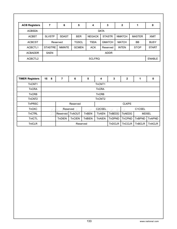 133
133
 134
134
 135
135
 136
136
 137
137
 138
138
 139
139
 140
140
 141
141
 142
142
 143
143
 144
144
 145
145
 146
146
 147
147
 148
148
 149
149
 150
150
 151
151
 152
152
 153
153
 154
154
 155
155
 156
156
