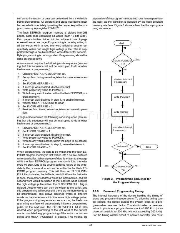
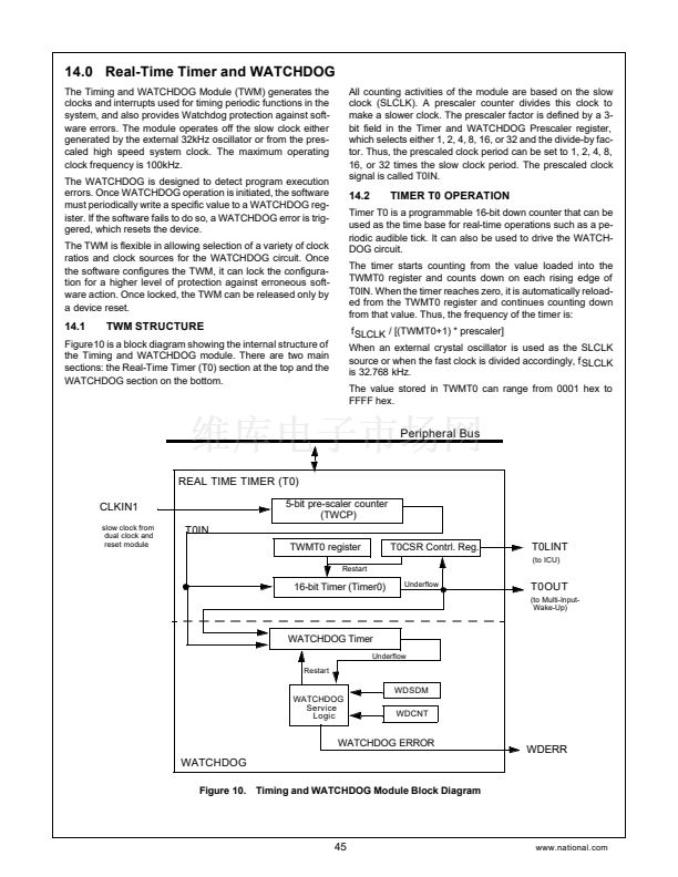
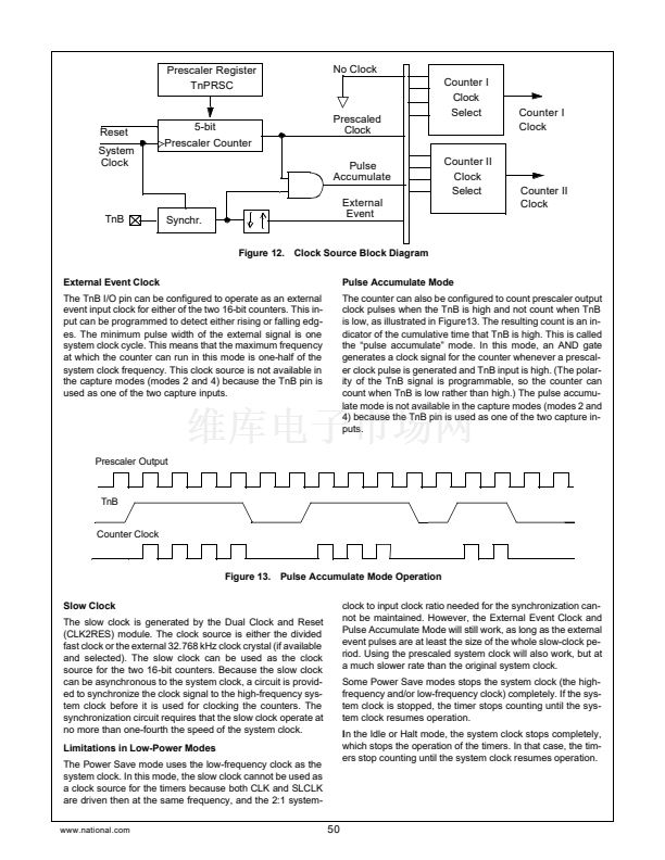
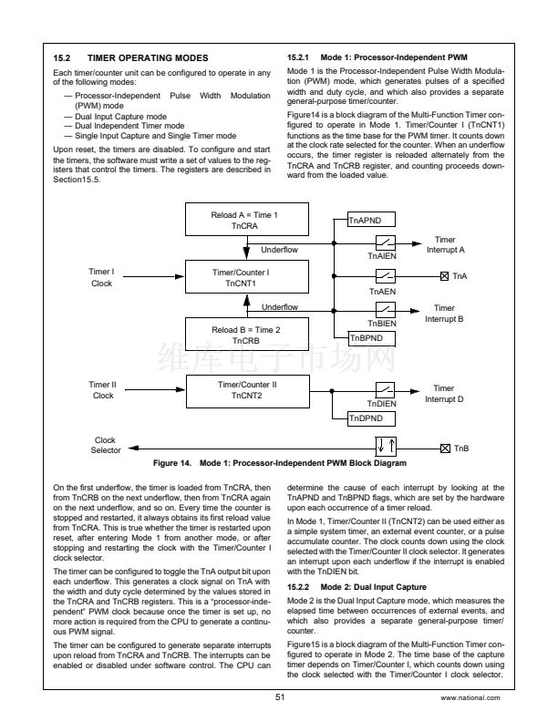
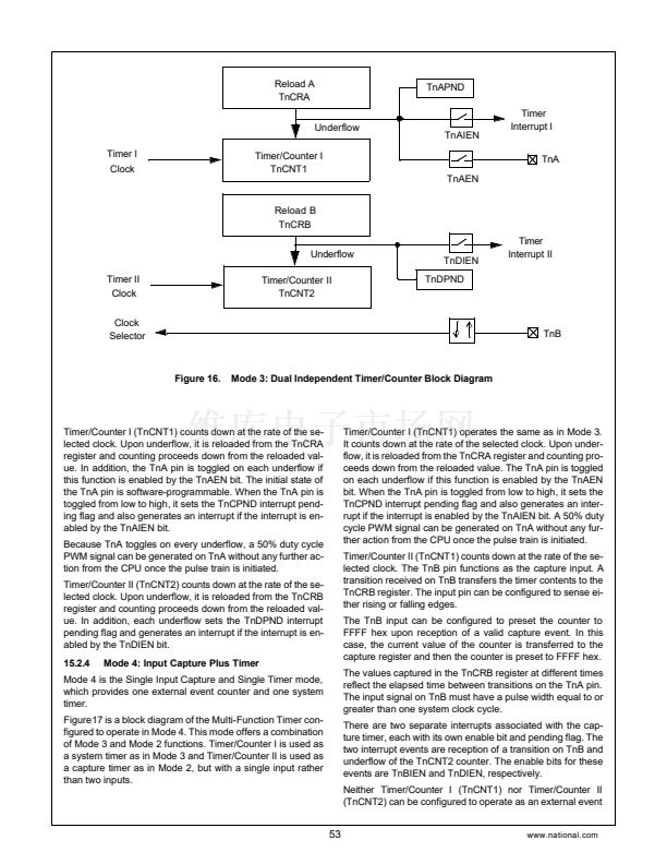
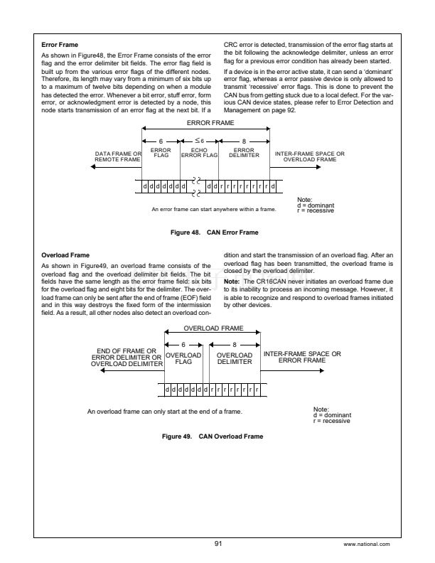
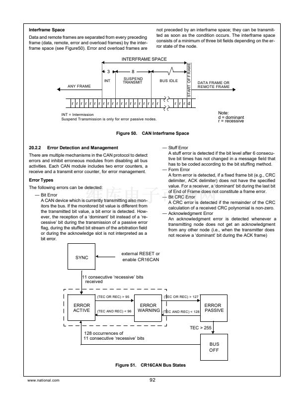
program the prescaler value in advance and leave it un-
changed while a program or erase operation is in progress.
A similar (but separate) prescaler factor is applied to the EE-
PROM data memory. See Section9.1.7 and Section9.3.4 for
details.
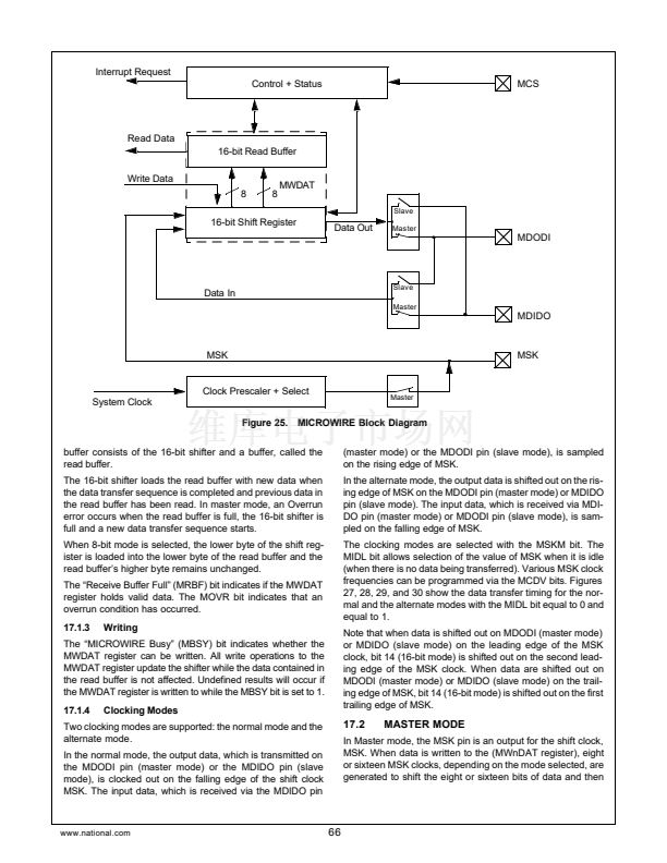
9.1.6
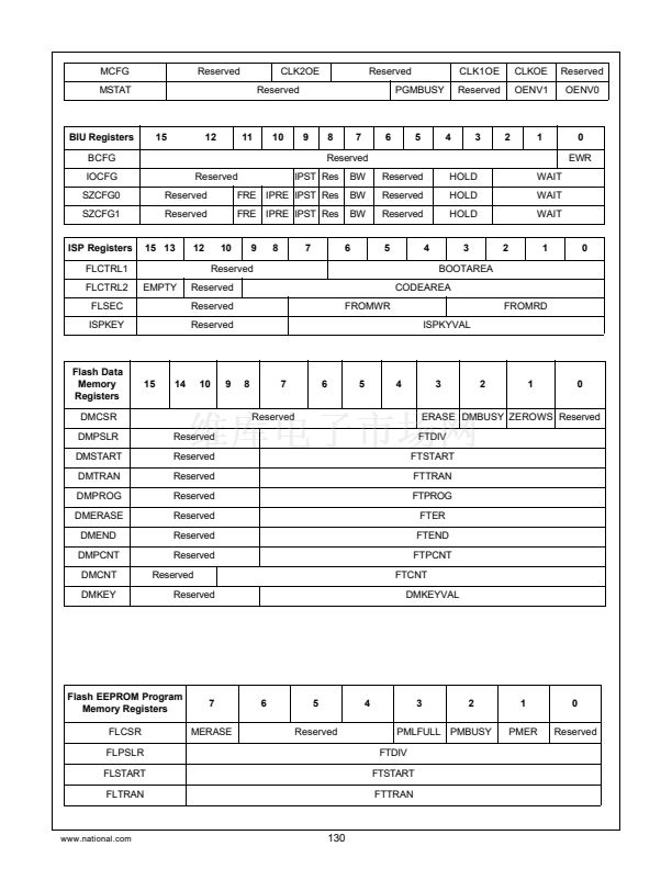
Flash EEPROM Program Memory Control and
Status Register (FLCSR)
12.5 MHz / (62+1) = 198.4 kHz. Do not modify this register
while a flash EEPROM program or erase operation is in
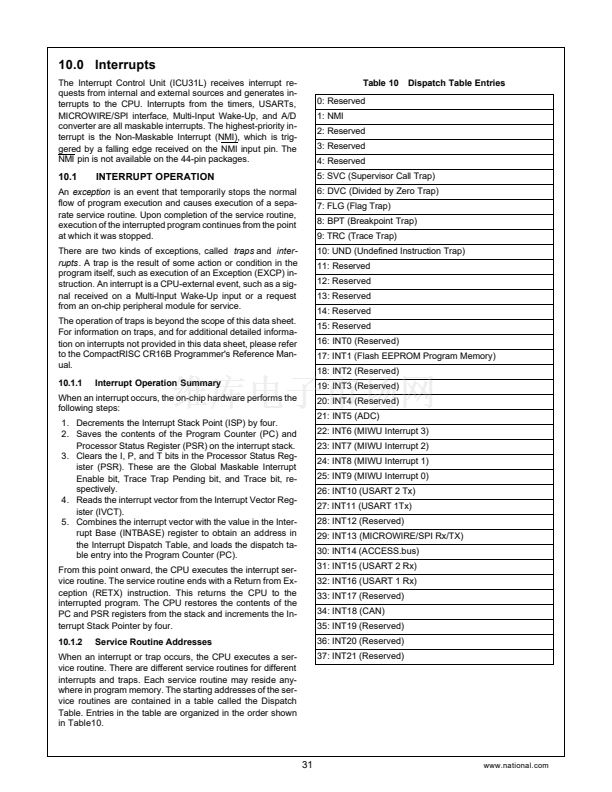
progress.
Upon reset, this register is programmed by default with the
value 63 hex (99 decimal), which is an appropriate setting for
a 20 MHz system clock.
9.1.8
Program Memory Start Time Reload (FLSTART)
The Flash EEPROM Program Memory Control and Status
(FLCSR) register is a byte-wide, read/write register that con-
tains several status and control bits related to the program
memory. All reserved bits must be written with 0 for the mem-
ory to operate properly when writing to this register. Upon re-
set, this register is cleared to zero when the flash memory on
the chip is in the idle state.
The register format is shown below.
7
MERASE
6
Reserved
4
3
PMLFULL
2
PMBUSY
1
PMER
0
Reserved
The FLSTART register is a byte-wide read/write register that
controls the program and erase start delay time. This value
is loaded into the lower 8 bits of the flash timing counter, and
at the same time, 00
2
is loaded into the upper 2 bits. Before
you program or erase the program memory for the first time,
program the FLSTART register with the proper prescaler val-
ue, FTSTART. The flash timing counter generates a delay of
(FTSTART+1) prescaler output clocks. The default value
provides a delay time of 10
碌s
when the prescaler output
clock is 200kHz. Do not modify this register while a program
or erase operation is in progress.
Upon reset, this register resets to 01
16
when the flash mem-
ory on the chip is in an idle state.
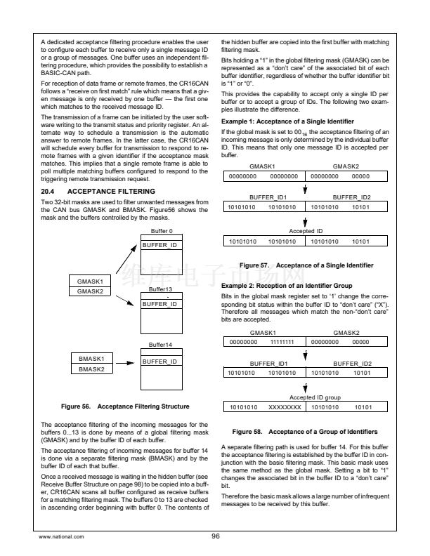
9.1.9
Program Memory Transition Time Reload
Register (FLTRAN)
PMER
PMBUSY
PMLFULL
MERASE
Flash EEPROM Program Memory page erase.
When set (1) with MERASE bit cleared, a valid
write to the flash EEPROM program memory
erases the entire flash EEPROM program
memory page pointed to by the write address
rather than performing a write to the addressed
memory location.
Program Memory Busy. This bit is automatical-
ly set to 1 when the flash EEPROM program
memory is busy being programmed, and
cleared to 0 at all other times. (The MSTAT.PG-
MBUSY is also set to 1 whenever the PMBUSY
bit is set to 1.)
Program Memory Write-Latch Buffer Full.
When set (1), the double-buffered data register
for program memory write operations is full.
When cleared (0), the double-buffered data
register is not full.
Mass Erase Flash EEPROM Program Memory
Array. When set (1) in ISP or test mode, a valid
write to the flash EEPROM program memory
performs an erase to the whole flash EEPROM
program memory rather than perform a write to
the addressed memory location. However, it is
necessary to enter new values into the
FLERASE and FLEND registers to adjust the
mass erase timing before starting the mass
erase.
The FLTRAN register is a byte-wide read/write register that
controls some program/erase transition times. This value is
loaded into the lower 8 bits of the flash timing counter, and at
the same time, 00
2
is loaded into the upper 2 bits. Before you
program or erase the program memory for the first time, you
should program the FLTRAM register with the proper pres-
caler value, FTTRAN. The flash timing counter generates a
delay of (FTTRAN + 1) prescaler output clocks. The default
value provides a delay time of 5碌s when the prescaler output
clock is 200kHz. Do not modify this register while a program
or erase operation is in progress.
Upon reset, this register resets to 00
1 6
when the flash mem-
ory on the chip is in an idle state.
9.1.10
Program Memory Programming Time Reload
Register (FLPROG)
9.1.7
Program Memory Timing Prescaler Register
(FLPSLR)
The FLPSLR register is a byte-wide, read/write register that
selects the prescaler divider ratio for the flash EEPROM pro-
gram memory programming clock. Before you program or
erase the program memory for the first time, you should pro-
gram the FLPSLR register with the proper prescaler value,
an 8-bit value called FTDIV. The device divides the system
clock by (FTDIV+1) to produce the program memory pro-
gramming clock.
You should choose a value of FTDIV to produce a clock of the
highest possible frequency that is equal to or just less than
200 kHz. For example, if the system clock frequency is 12.5
MHz, use the value 3E hex (62 decimal) for FTDIV, because
www.national.com
The FLPROG register is a byte-wide read/write register that
controls the programming pulse width. This value is loaded
into the lower 8 bits of the flash timing counter, and at the
same time, 00
2
is loaded into the upper 2 bits. Before you
program or erase the program memory for the first time, pro-
gram the FLPROG register with the proper prescaler value,
FTPROG. The flash timing counter generates a programming
pulse width of (FTPROG + 1) prescaler output clocks. The
default value provides a delay time of 30碌s when the prescal-
er output clock is 200kHz.
Do not modify this register while program/erase operation is
in progress.
Upon reset, this register resets to 05
1 6
when the flash mem-
ory on the chip is in idle state.
24


 1
1
 2
2
 3
3
 4
4
 5
5
 6
6
 7
7
 8
8
 9
9
 10
10
 11
11
 12
12
 13
13
 14
14
 15
15
 16
16
 17
17
 18
18
 19
19
 20
20
 21
21
 22
22
 23
23
 24
24
 25
25
 26
26
 27
27
 28
28
 29
29
 30
30
 31
31
 32
32
 33
33
 34
34
 35
35
 36
36
 37
37
 38
38
 39
39
 40
40
 41
41
 42
42
 43
43
 44
44
 45
45
 46
46
 47
47
 48
48
 49
49
 50
50
 51
51
 52
52
 53
53
 54
54
 55
55
 56
56
 57
57
 58
58
 59
59
 60
60
 61
61
 62
62
 63
63
 64
64
 65
65
 66
66
 67
67
 68
68
 69
69
 70
70
 71
71
 72
72
 73
73
 74
74
 75
75
 76
76
 77
77
 78
78
 79
79
 80
80
 81
81
 82
82
 83
83
 84
84
 85
85
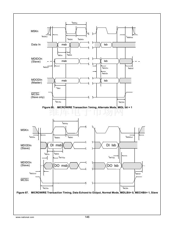
 86
86
 87
87
 88
88
 89
89
 90
90
 91
91
 92
92
 93
93
 94
94
 95
95
 96
96
 97
97
 98
98
 99
99
 100
100
 101
101
 102
102
 103
103
 104
104
 105
105
 106
106
 107
107
 108
108
 109
109
 110
110
 111
111
 112
112
 113
113
 114
114
 115
115
 116
116
 117
117
 118
118
 119
119
 120
120
 121
121
 122
122
 123
123
 124
124
 125
125
 126
126
 127
127
 128
128
 129
129
 130
130
 131
131
 132
132
 133
133
 134
134
 135
135
 136
136
 137
137
 138
138
 139
139
 140
140
 141
141
 142
142
 143
143
 144
144
 145
145
 146
146
 147
147
 148
148
 149
149
 150
150
 151
151
 152
152
 153
153
 154
154
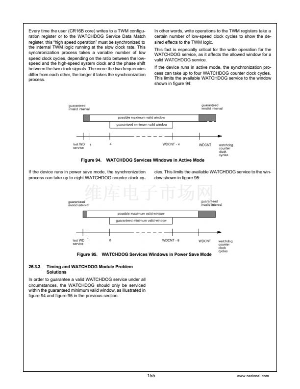 155
155
 156
156
