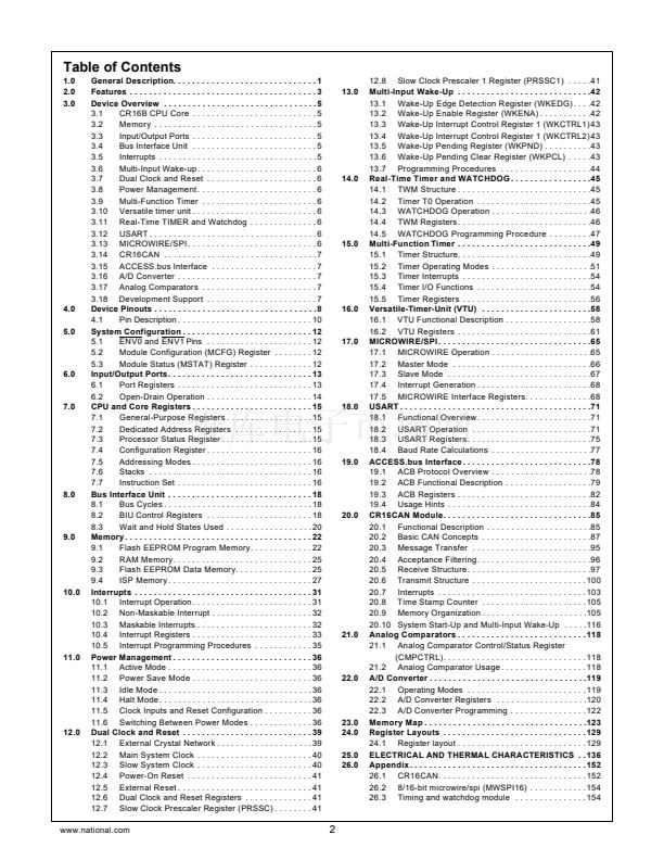
not permitted while ISP flash EEPROM program memory is
being programmed.
The ISP flash memory is divided into 192 pages, each page
containing 4 words (each 16 bits wide). Each page is further
divided into two rows. Erase is carried out one page at a time,
whereas programming is carried out one row (or one partial
row) at a time.
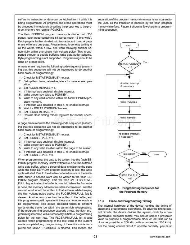
Once an erase or programming operation is started, the PG-
MBUSY bit in the MSTAT register is automatically set, and
then cleared when the operation is complete. All high-voltage
pulses and timing needed for programming and erasing are
provided internally. The program memory cannot be access-
ed while the PGMBUSY bit is set.
Erase Procedure
Erasing a page requires the following code sequence:
1.
2.
3.
4.
5.
6.
7.
Verify that the MSTAT.PGMBUSY bit is cleared.
Set the DMCSR.ERASE bit to 1.
Locally disable interrupts.
Write proper key value to the ISPKEY register.
Write to any valid page to be erased.
Re-enable interrupts disabled in Step 3.
Set the DMCSR.ERASE bit to 0.
Programming Procedure
through a byte write instruction when the write instruction is
anywhere within the user boot ROM area (defined above) ex-
cept for the last two words. When the user boot ROM area
has been disabled, this word cannot be programmed in the
IRE environment. Note that when this word is erased for re-
programming, the other words in the same page must first be
saved, and then re-programmed.
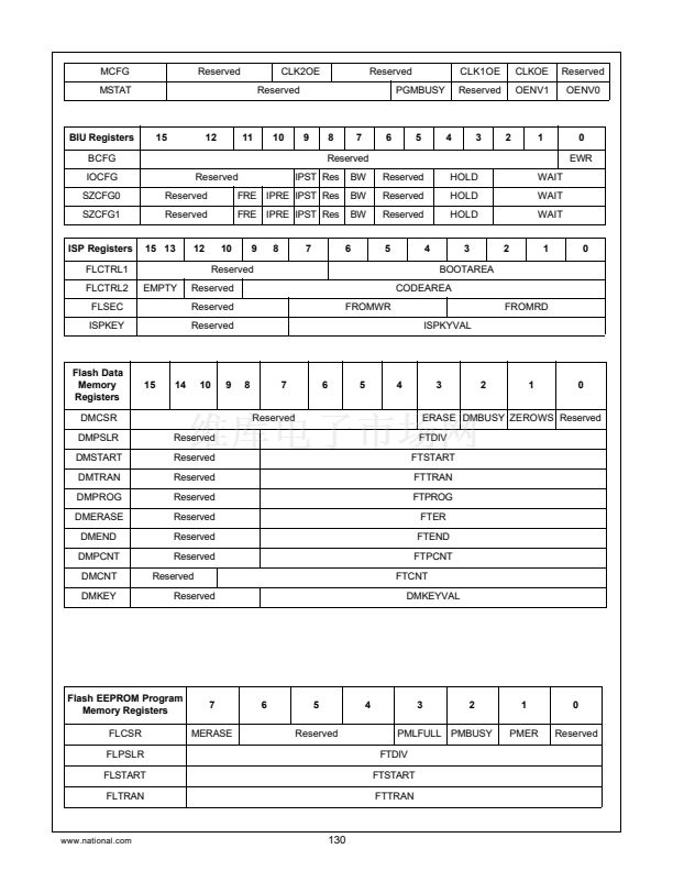
7
EMPTY
5
4
2
1
0
Reserved
CODEAREA[9:8]
9.4.3
Programming is done by writing one byte or word at a time
and should be done on already erased memory.
Programming the ISP flash EEPROM program memory re-
quires the following code sequence:
1.
2.
3.
4.
5.
Verify that the MSTAT.PGMBUSY bit is cleared.
Locally disable interrupts.
Write proper key value to the ISPKEY register.
Write a byte or word to the addressed location.
Re-enable interrupts disabled in Step 2.
CODEAREA[9:8]
The 2 least significant bits in address E5FE
contains the two most significant bits of the 10-
bit CODEAREA field. The description of
CODEAREA is shown in the E5FC section.
EMPTY
The EMPTY status indicates if the flash EE-
PROM program memory array is empty or not.
It is located in the 3 most significant bits in ad-
dress E5FE. When two or more bits in the
EMPTY field are set, the flash EEPROM pro-
gram memory is empty. Upon reset of the de-
vice and the environment select pins are all
high, the device operates in ISP environment
rather than IRE environment. After the program
memory has been filled with user code, this
field should be cleared to 000
2
.
000, 001, 010, 100: Program memory contains user code
011, 101, 11x: Program memory is empty, do not start up in IRE
E5FF Byte
Upon reset, the byte located in the E5FF address is read into
the FLSEC register. This byte cannot be written to in the IRE
environment. The format of the E5FF byte is shown below:
7
FROMWR
4
3
FROMRD
0
Programmed values can be verified through normal read op-
erations.
If a reset occurs in the middle of an erase or programming
operation, the operation is terminated. The reset is extended
until the flash EEPROM memory returns to the idle state.
9.4.4
Erase and Programming Timing
The FROMRD and FROMWR fields in address location
E5FF respectively provide read and write security to the flash
EEPROM program memory array while executing instruc-
tions in all environments except IRE. The user should always
write 0000
2
to enable security feature.
0000, 0001, 0010, 0100, 1000: Security feature enabled
0011, 0101, 011x, 1001, 101x, 11xx: Security feature disabled
The program and erase timing are controlled by the flash EE-
PROM data memory logic.
9.4.5
Memory Control and Protection Features
FROMRD
The last 8 bytes of the ISP memory are reserved for special
functions and some of these bytes provide memory protec-
tion and security for the flash EEPROM program memory.
Read and various types of write protection are provided.
During the reset stretch period, bytes located at E5FE and
E5FF are read out to the FLCTRL2 and FLSEC registers re-
spectively. Upon reset and before an instruction fetch, bytes
located at E5FC and E5FD are read out to the FLCTRL2 and
FLCTRL1 registers respectively. Parts of FLCTRL2 register
are loaded at different times.
E5FE Byte
Upon reset of the chip, the byte located at E5FE is read into
the FLCTRL2 register. It can be written in the ISP or test en-
vironments. It can also be written in the IRE environment
www.national.com
FROMWR
Upon reset of the chip, read security is enabled
and 0000 is returned in all environments except
IRE. The internal program code can only be ex-
ecuted in the IRE environment when read se-
curity is activated.
Upon reset of the chip, write security is enabled
and program and erase operations to the flash
EEPROM program memory in either program-
ming modes are prevented.
Once read/write security is enabled, the odd numbered bytes
from address E5F9 to E5FF cannot be erased. Once a secu-
rity feature has been enabled, it cannot be undone. To pre-
vent the security status from being erased, the ISP and data
memory array cannot be mass erased.
Note:
In flash memory test mode, this condition also pre-
vents the odd numbered bytes of the high endurance flash
EEPROM data memory (F001 to F07F) from being erased;
28


 1
1
 2
2
 3
3
 4
4
 5
5
 6
6
 7
7
 8
8
 9
9
 10
10
 11
11
 12
12
 13
13
 14
14
 15
15
 16
16
 17
17
 18
18
 19
19
 20
20
 21
21
 22
22
 23
23
 24
24
 25
25
 26
26
 27
27
 28
28
 29
29
 30
30
 31
31
 32
32
 33
33
 34
34
 35
35
 36
36
 37
37
 38
38
 39
39
 40
40
 41
41
 42
42
 43
43
 44
44
 45
45
 46
46
 47
47
 48
48
 49
49
 50
50
 51
51
 52
52
 53
53
 54
54
 55
55
 56
56
 57
57
 58
58
 59
59
 60
60
 61
61
 62
62
 63
63
 64
64
 65
65
 66
66
 67
67
 68
68
 69
69
 70
70
 71
71
 72
72
 73
73
 74
74
 75
75
 76
76
 77
77
 78
78
 79
79
 80
80
 81
81
 82
82
 83
83
 84
84
 85
85
 86
86
 87
87
 88
88
 89
89
 90
90
 91
91
 92
92
 93
93
 94
94
 95
95
 96
96
 97
97
 98
98
 99
99
 100
100
 101
101
 102
102
 103
103
 104
104
 105
105
 106
106
 107
107
 108
108
 109
109
 110
110
 111
111
 112
112
 113
113
 114
114
 115
115
 116
116
 117
117
 118
118
 119
119
 120
120
 121
121
 122
122
 123
123
 124
124
 125
125
 126
126
 127
127
 128
128
 129
129
 130
130
 131
131
 132
132
 133
133
 134
134
 135
135
 136
136
 137
137
 138
138
 139
139
 140
140
 141
141
 142
142
 143
143
 144
144
 145
145
 146
146
 147
147
 148
148
 149
149
 150
150
 151
151
 152
152
 153
153
 154
154
 155
155
 156
156
