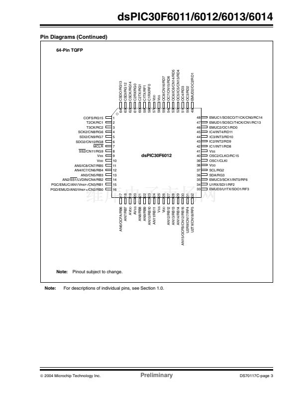
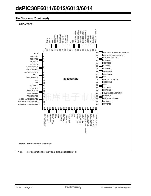
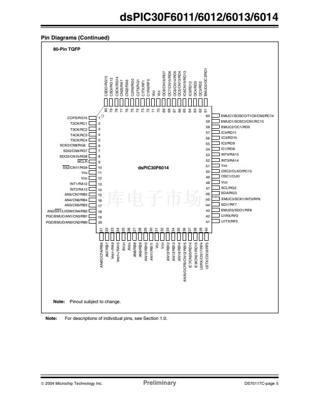
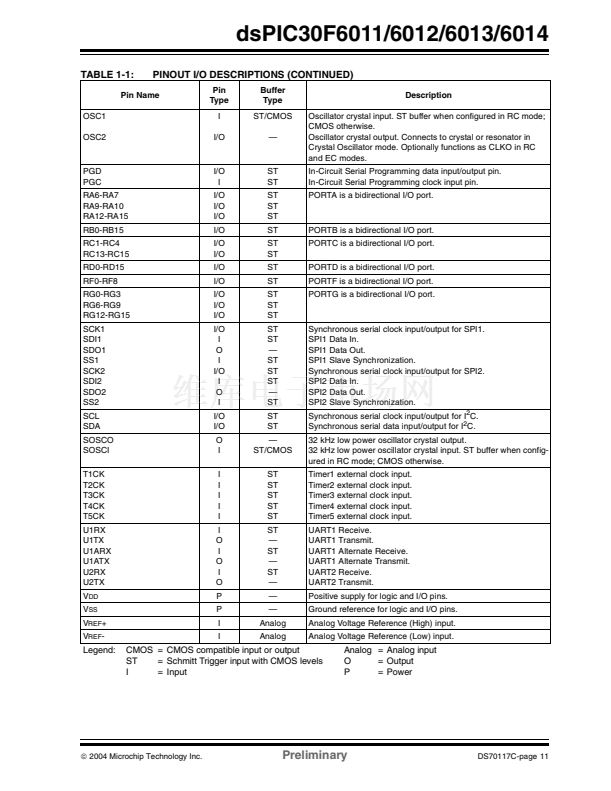
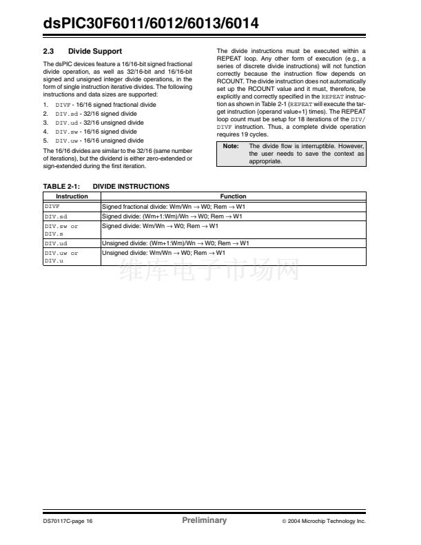
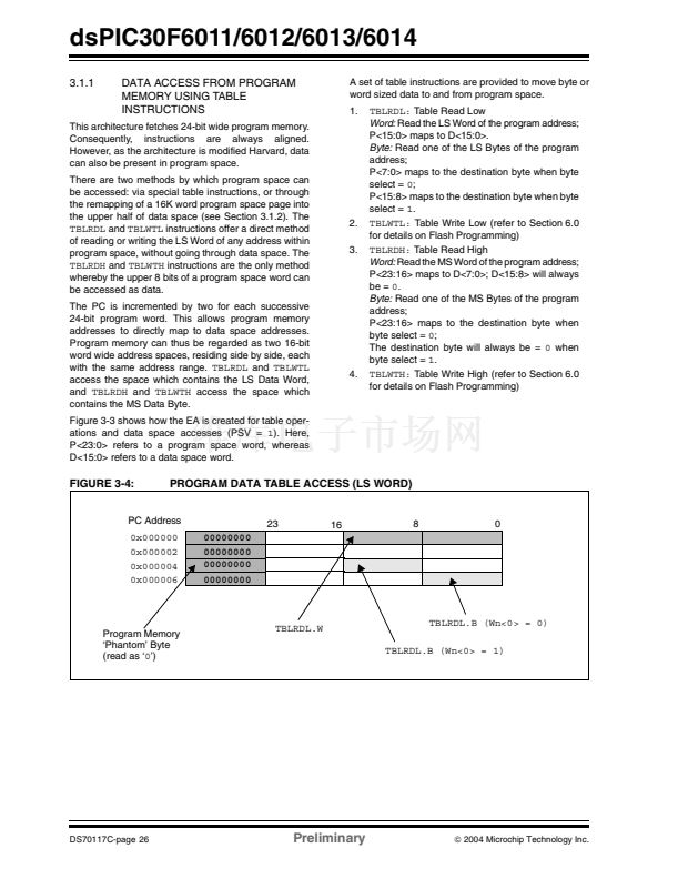
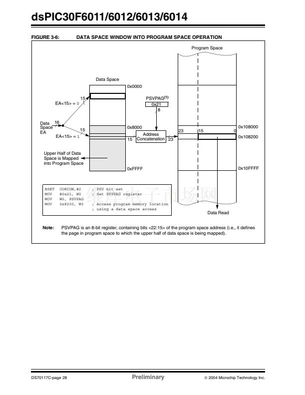
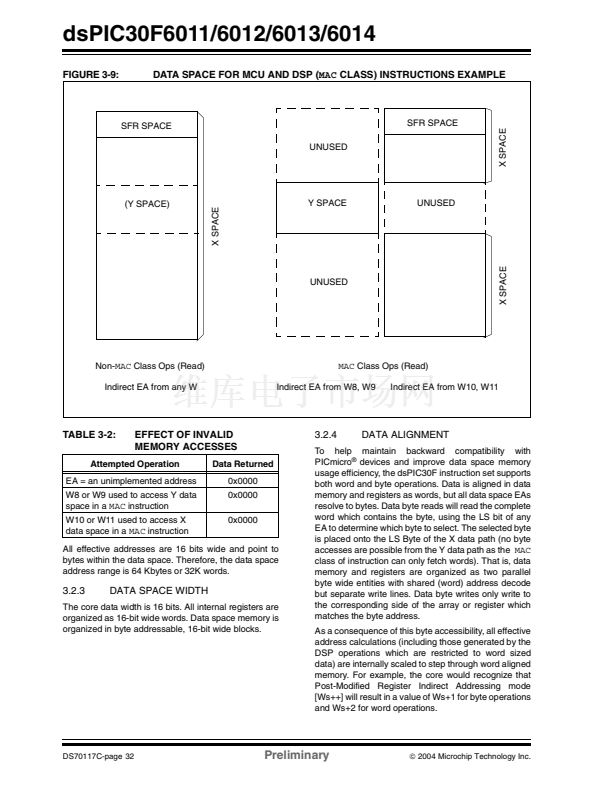
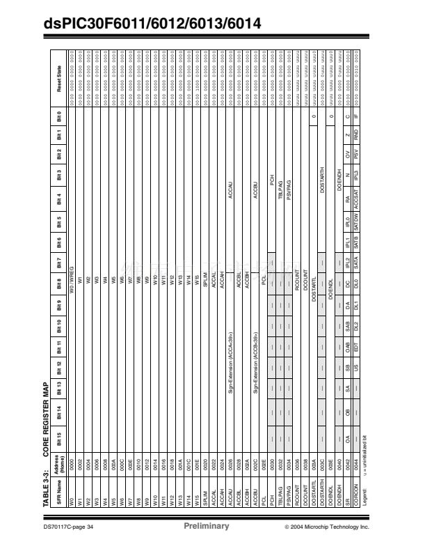
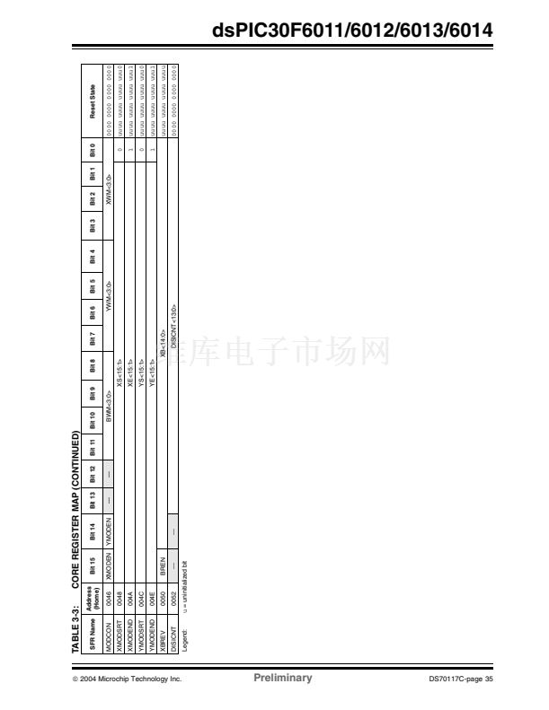
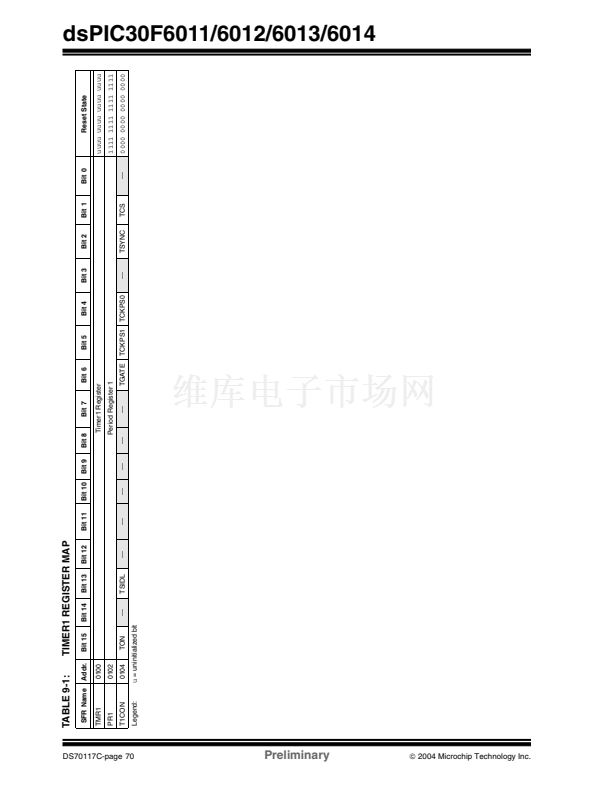
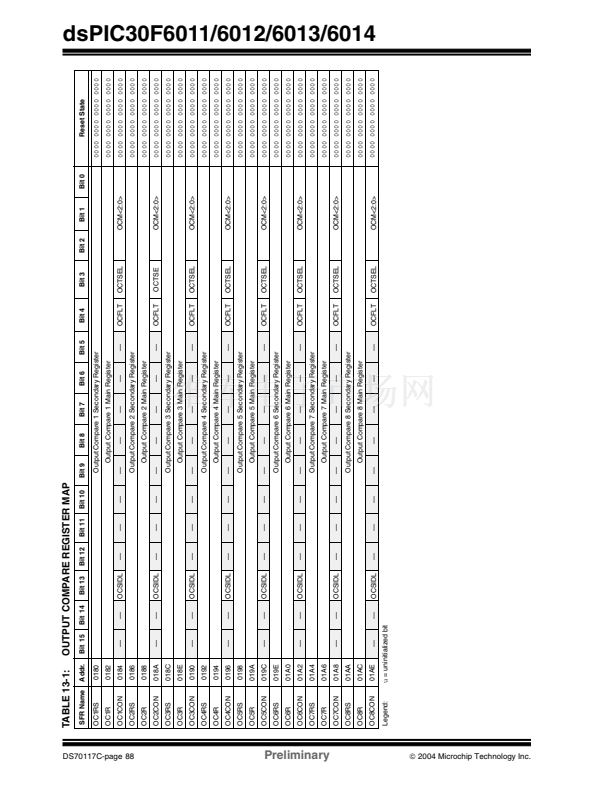
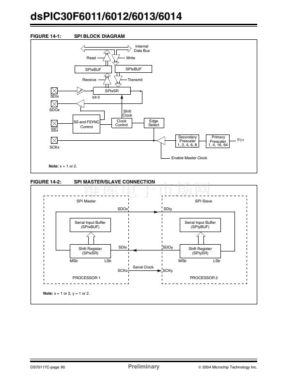
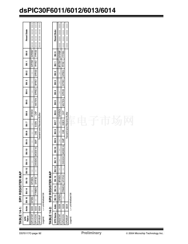
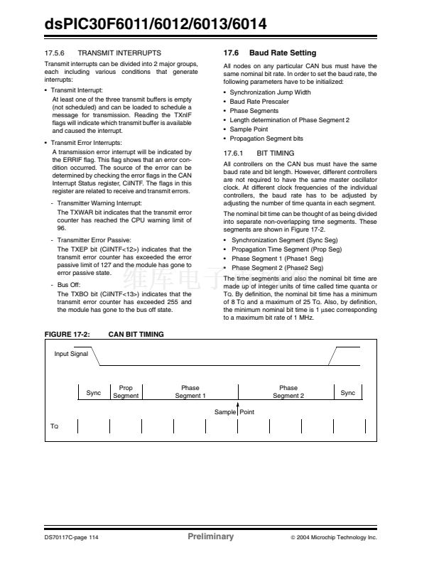
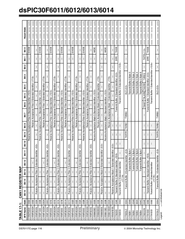
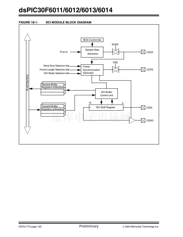
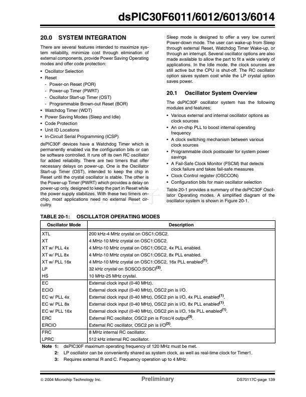
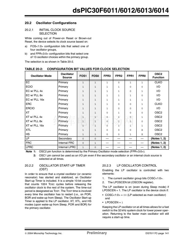
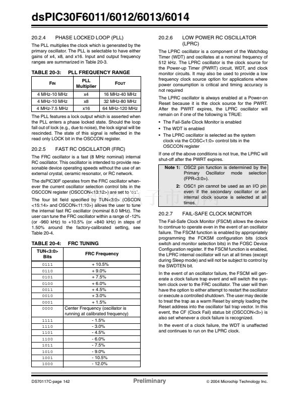
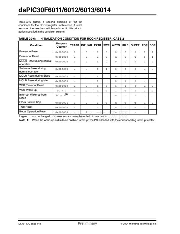
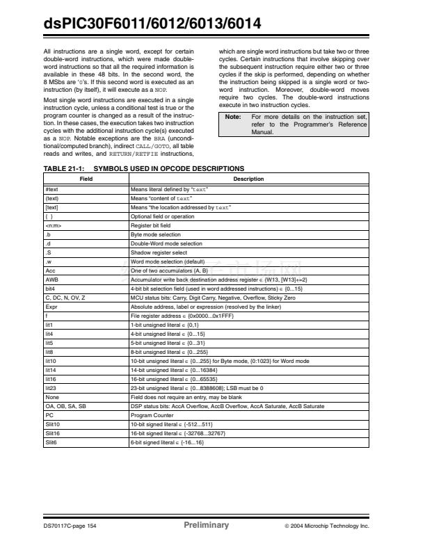
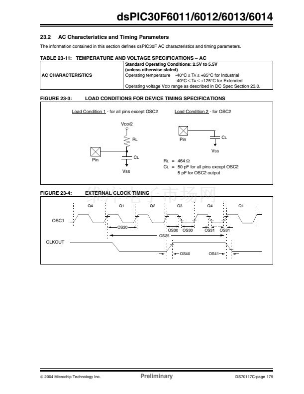
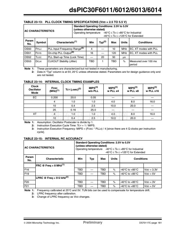
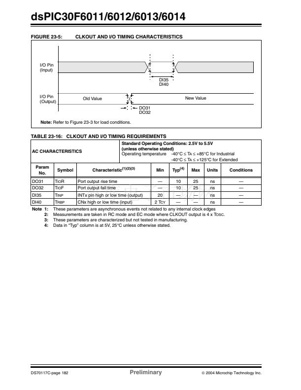
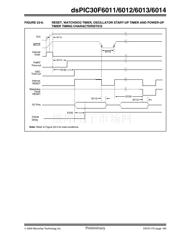
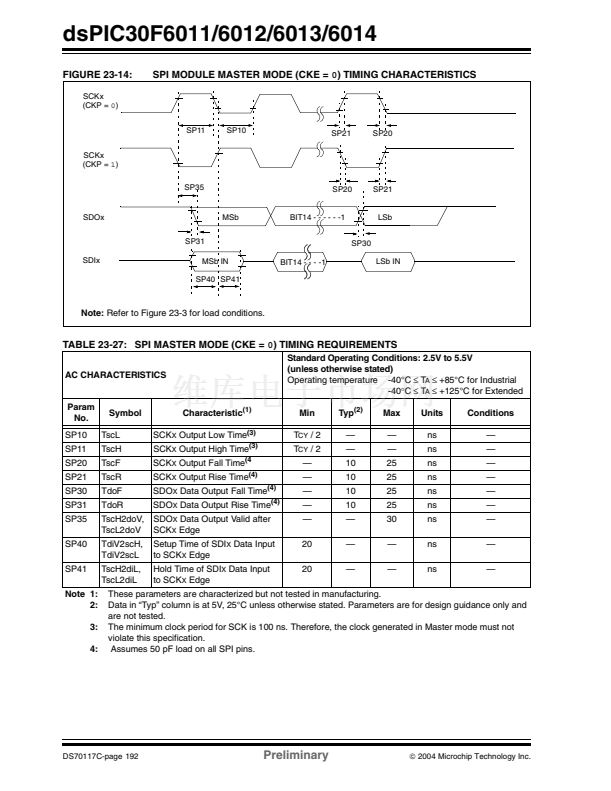
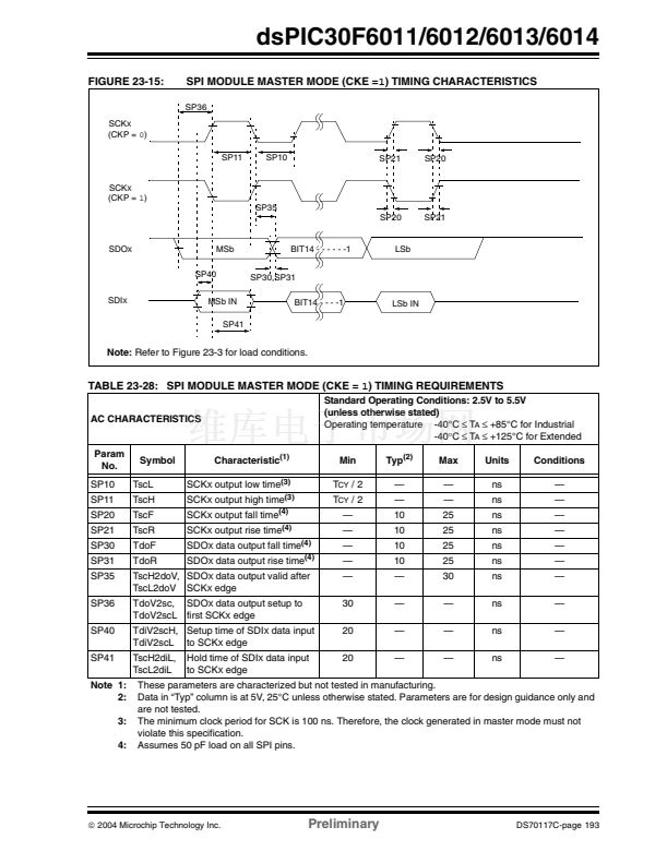
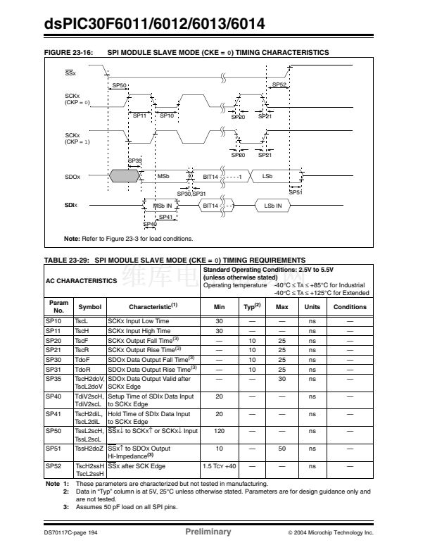
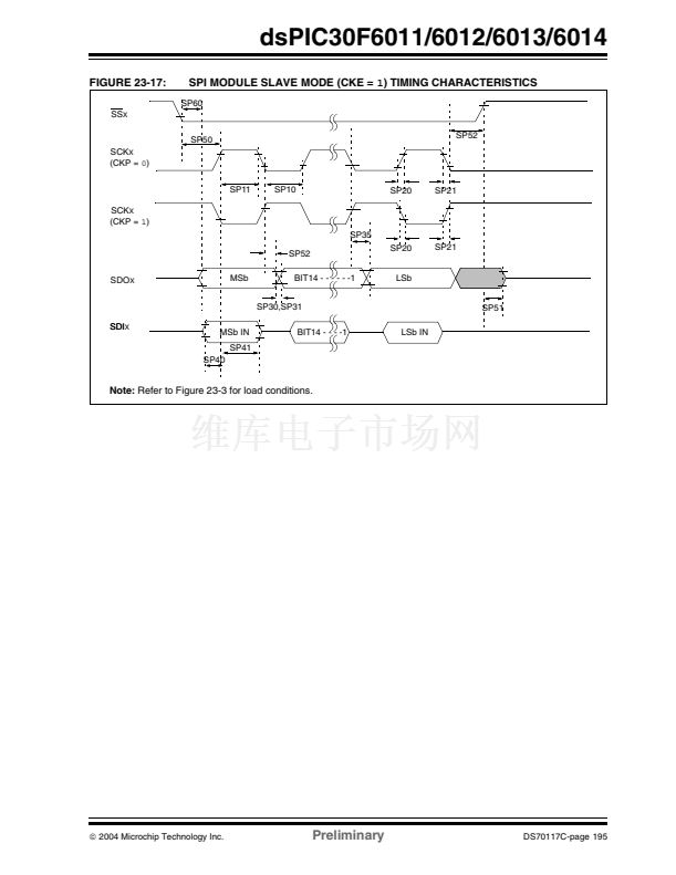
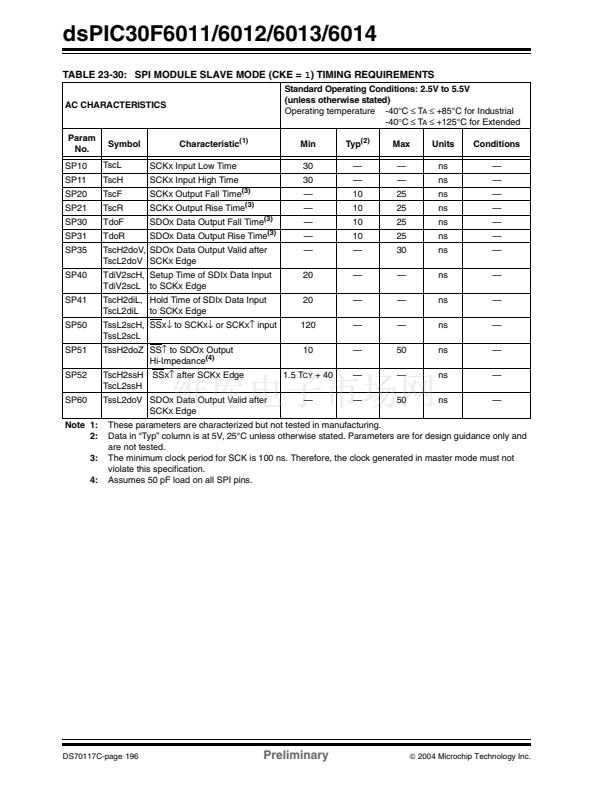
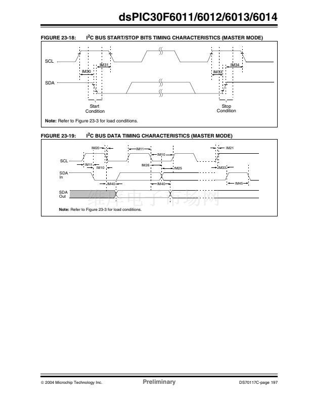
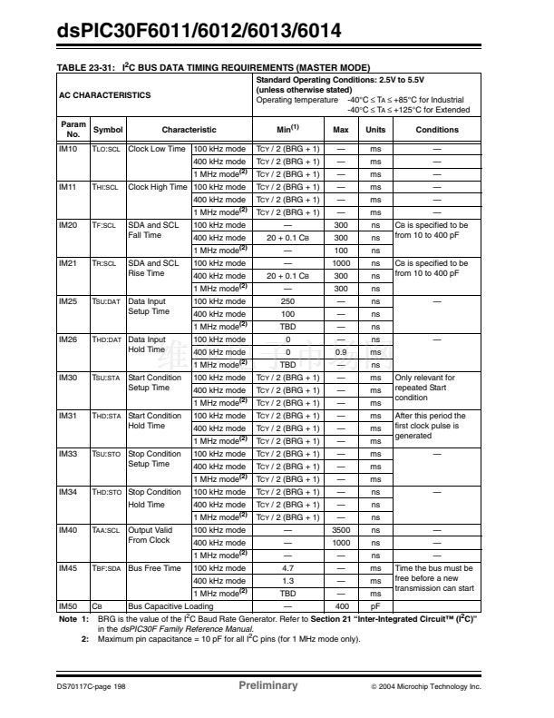
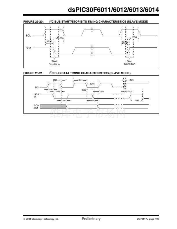
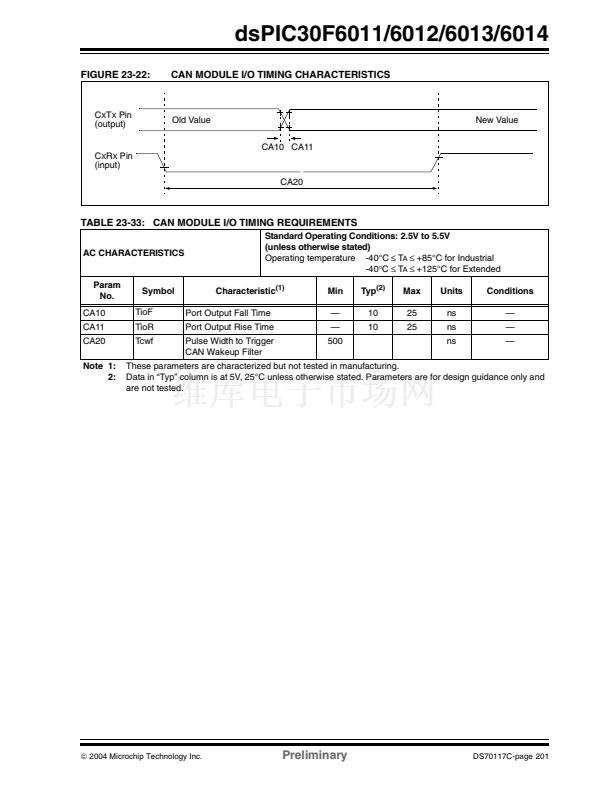
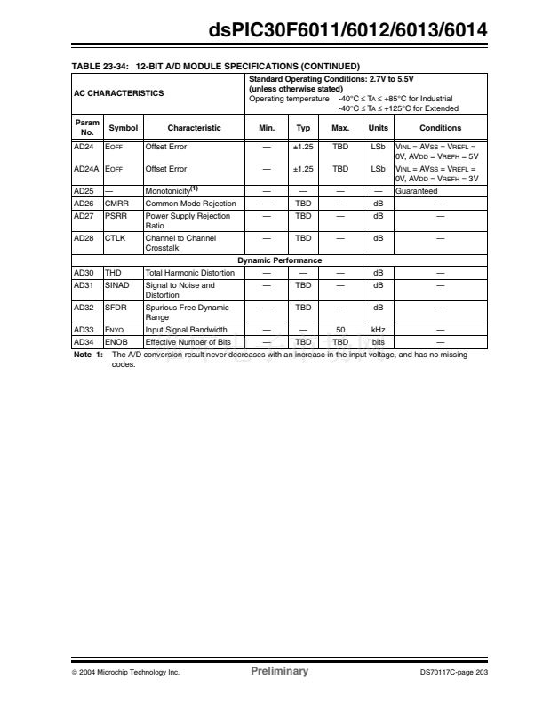
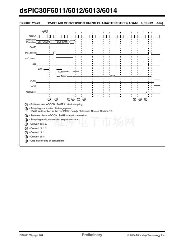
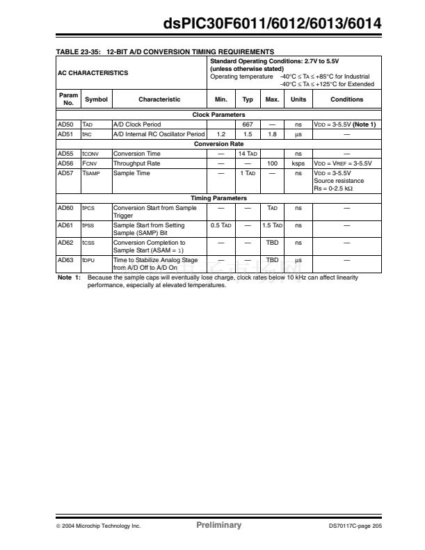
dsPIC30F6011/6012/6013/6014
All word accesses must be aligned to an even address.
Misaligned word data fetches are not supported so
care must be taken when mixing byte and word opera-
tions, or translating from 8-bit MCU code. Should a mis-
aligned read or write be attempted, an address error
trap will be generated. If the error occurred on a read,
the instruction underway is completed, whereas if it
occurred on a write, the instruction will be executed but
the write will not occur. In either case, a trap will then
be executed, allowing the system and/or user to exam-
ine the machine state prior to execution of the address
fault.
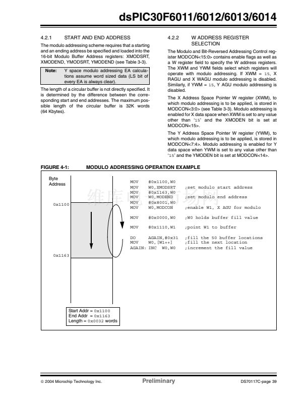
3.2.6
SOFTWARE STACK
The dsPIC devices contain a software stack. W15 is
used as the stack pointer.
The stack pointer always points to the first available
free word and grows from lower addresses towards
higher addresses. It pre-decrements for stack pops and
post-increments for stack pushes as shown in Figure 3-
11. Note that for a PC push during any
CALL
instruc-
tion, the MSB of the PC is zero-extended before the
push, ensuring that the MSB is always clear.
Note:
A PC push during exception processing
will concatenate the SRL register to the
MSB of the PC prior to the push.
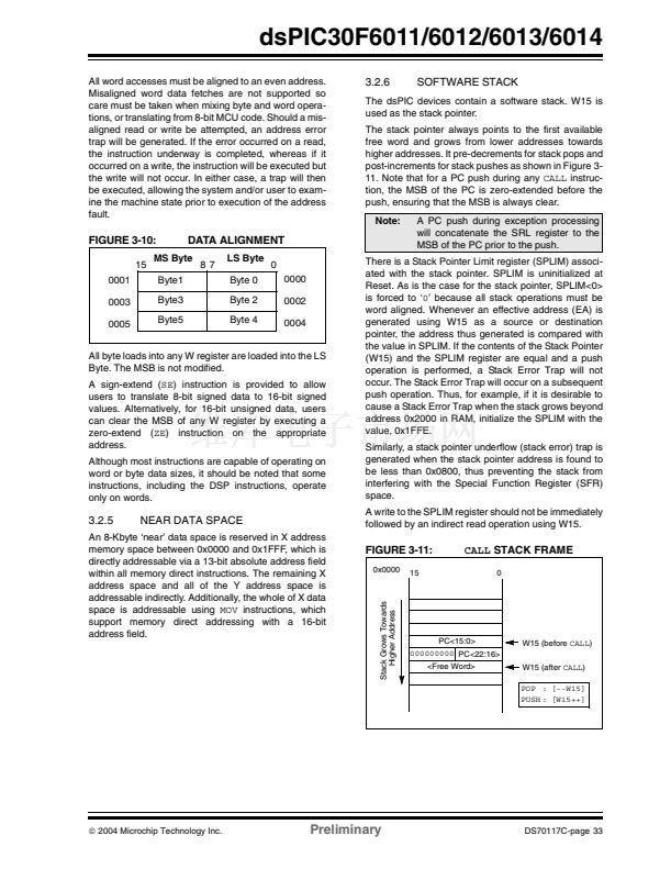
FIGURE 3-10:
15
0001
0003
0005
DATA ALIGNMENT
87
LS Byte
Byte 0
Byte 2
Byte 4
0
0000
0002
0004
MS Byte
Byte1
Byte3
Byte5
All byte loads into any W register are loaded into the LS
Byte. The MSB is not modified.
A sign-extend (SE) instruction is provided to allow
users to translate 8-bit signed data to 16-bit signed
values. Alternatively, for 16-bit unsigned data, users
can clear the MSB of any W register by executing a
zero-extend (ZE) instruction on the appropriate
address.
Although most instructions are capable of operating on
word or byte data sizes, it should be noted that some
instructions, including the DSP instructions, operate
only on words.
There is a Stack Pointer Limit register (SPLIM) associ-
ated with the stack pointer. SPLIM is uninitialized at
Reset. As is the case for the stack pointer, SPLIM<0>
is forced to 鈥?鈥?because all stack operations must be
word aligned. Whenever an effective address (EA) is
generated using W15 as a source or destination
pointer, the address thus generated is compared with
the value in SPLIM. If the contents of the Stack Pointer
(W15) and the SPLIM register are equal and a push
operation is performed, a Stack Error Trap will not
occur. The Stack Error Trap will occur on a subsequent
push operation. Thus, for example, if it is desirable to
cause a Stack Error Trap when the stack grows beyond
address 0x2000 in RAM, initialize the SPLIM with the
value, 0x1FFE.
Similarly, a stack pointer underflow (stack error) trap is
generated when the stack pointer address is found to
be less than 0x0800, thus preventing the stack from
interfering with the Special Function Register (SFR)
space.
A write to the SPLIM register should not be immediately
followed by an indirect read operation using W15.
3.2.5
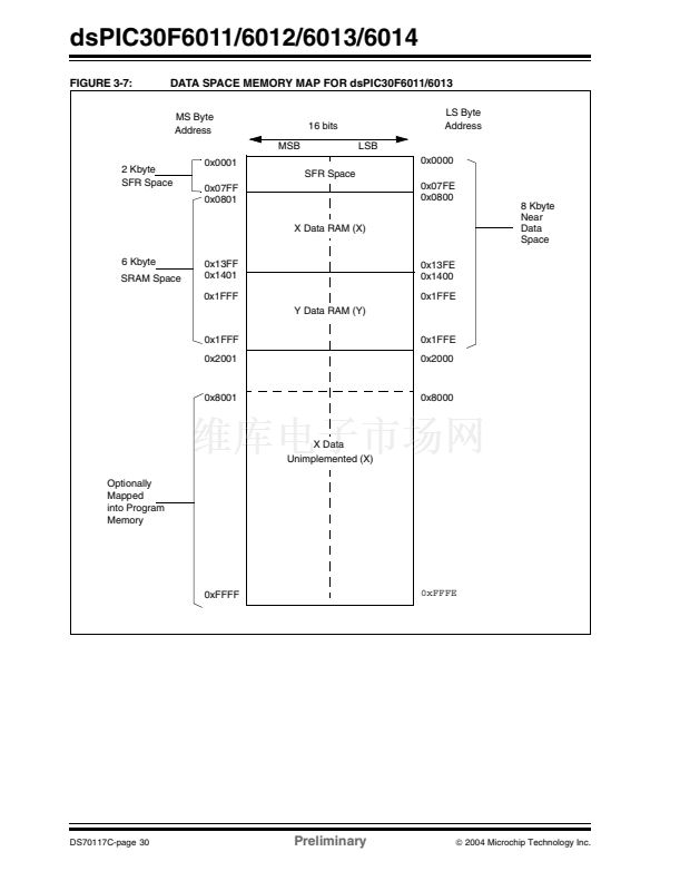
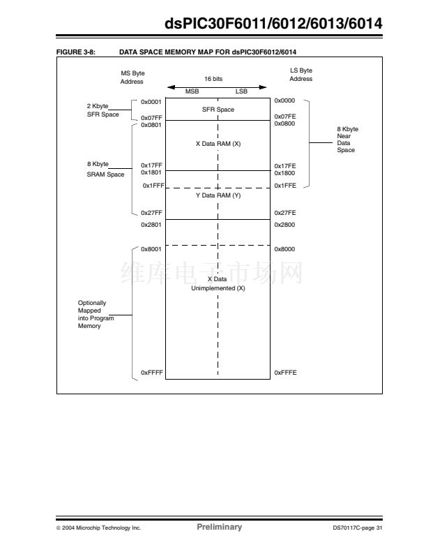
NEAR DATA SPACE
Stack Grows Towards
Higher Address
An 8-Kbyte 鈥榥ear鈥?data space is reserved in X address
memory space between 0x0000 and 0x1FFF, which is
directly addressable via a 13-bit absolute address field
within all memory direct instructions. The remaining X
address space and all of the Y address space is
addressable indirectly. Additionally, the whole of X data
space is addressable using
MOV
instructions, which
support memory direct addressing with a 16-bit
address field.
FIGURE 3-11:
0x0000
15
CALL
STACK FRAME
0
PC<15:0>
000000000
PC<22:16>
<Free Word>
W15 (before
CALL)
W15 (after
CALL)
POP : [--W15]
PUSH : [W15++]
铮?/div>
2004 Microchip Technology Inc.
Preliminary
DS70117C-page 33


 1
1
 2
2
 3
3
 4
4
 5
5
 6
6
 7
7
 8
8
 9
9
 10
10
 11
11
 12
12
 13
13
 14
14
 15
15
 16
16
 17
17
 18
18
 19
19
 20
20
 21
21
 22
22
 23
23
 24
24
 25
25
 26
26
 27
27
 28
28
 29
29
 30
30
 31
31
 32
32
 33
33
 34
34
 35
35
 36
36
 37
37
 38
38
 39
39
 40
40
 41
41
 42
42
 43
43
 44
44
 45
45
 46
46
 47
47
 48
48
 49
49
 50
50
 51
51
 52
52
 53
53
 54
54
 55
55
 56
56
 57
57
 58
58
 59
59
 60
60
 61
61
 62
62
 63
63
 64
64
 65
65
 66
66
 67
67
 68
68
 69
69
 70
70
 71
71
 72
72
 73
73
 74
74
 75
75
 76
76
 77
77
 78
78
 79
79
 80
80
 81
81
 82
82
 83
83
 84
84
 85
85
 86
86
 87
87
 88
88
 89
89
 90
90
 91
91
 92
92
 93
93
 94
94
 95
95
 96
96
 97
97
 98
98
 99
99
 100
100
 101
101
 102
102
 103
103
 104
104
 105
105
 106
106
 107
107
 108
108
 109
109
 110
110
 111
111
 112
112
 113
113
 114
114
 115
115
 116
116
 117
117
 118
118
 119
119
 120
120
 121
121
 122
122
 123
123
 124
124
 125
125
 126
126
 127
127
 128
128
 129
129
 130
130
 131
131
 132
132
 133
133
 134
134
 135
135
 136
136
 137
137
 138
138
 139
139
 140
140
 141
141
 142
142
 143
143
 144
144
 145
145
 146
146
 147
147
 148
148
 149
149
 150
150
 151
151
 152
152
 153
153
 154
154
 155
155
 156
156
 157
157
 158
158
 159
159
 160
160
 161
161
 162
162
 163
163
 164
164
 165
165
 166
166
 167
167
 168
168
 169
169
 170
170
 171
171
 172
172
 173
173
 174
174
 175
175
 176
176
 177
177
 178
178
 179
179
 180
180
 181
181
 182
182
 183
183
 184
184
 185
185
 186
186
 187
187
 188
188
 189
189
 190
190
 191
191
 192
192
 193
193
 194
194
 195
195
 196
196
 197
197
 198
198
 199
199
 200
200
 201
201
 202
202
 203
203
 204
204
 205
205
 206
206
 207
207
 208
208
 209
209
 210
210
 211
211
 212
212
 213
213
 214
214
 215
215
 216
216
 217
217
 218
218
 219
219
 220
220
 221
221
 222
222
