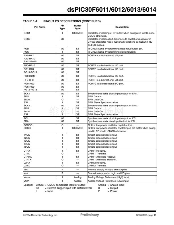
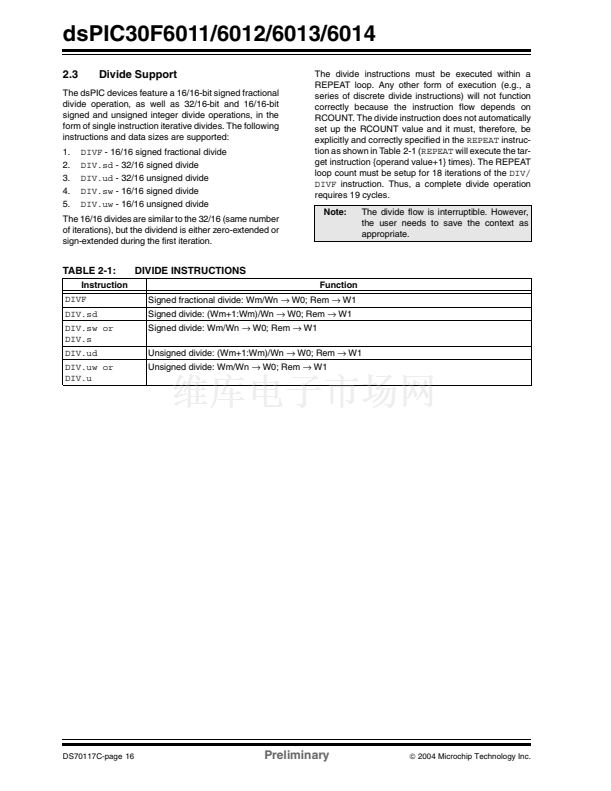
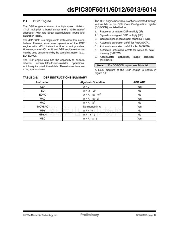
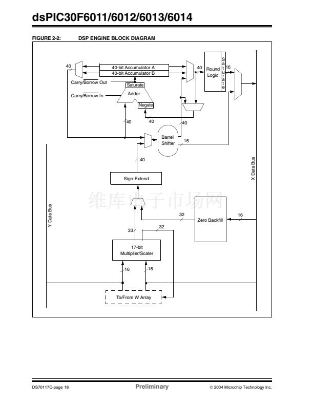
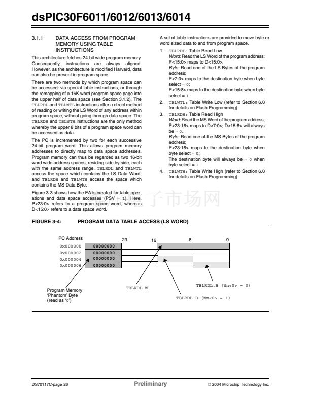
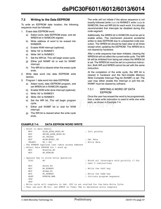
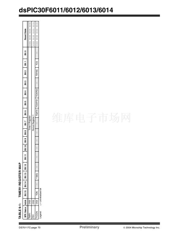
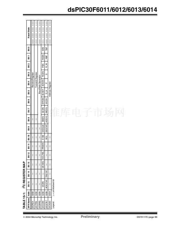
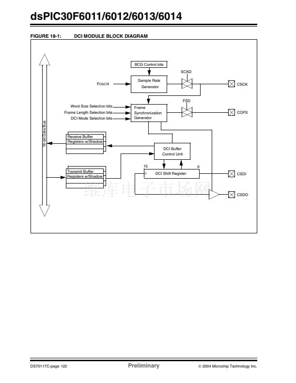
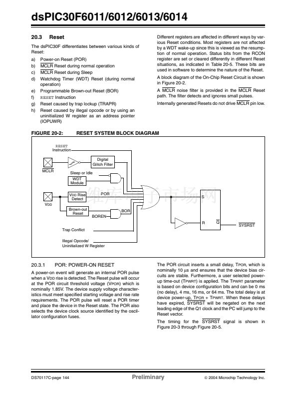
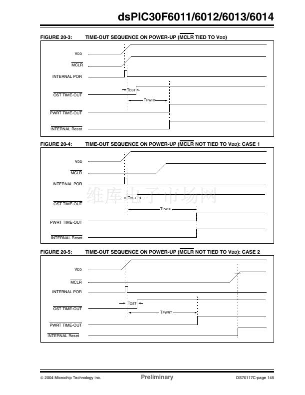
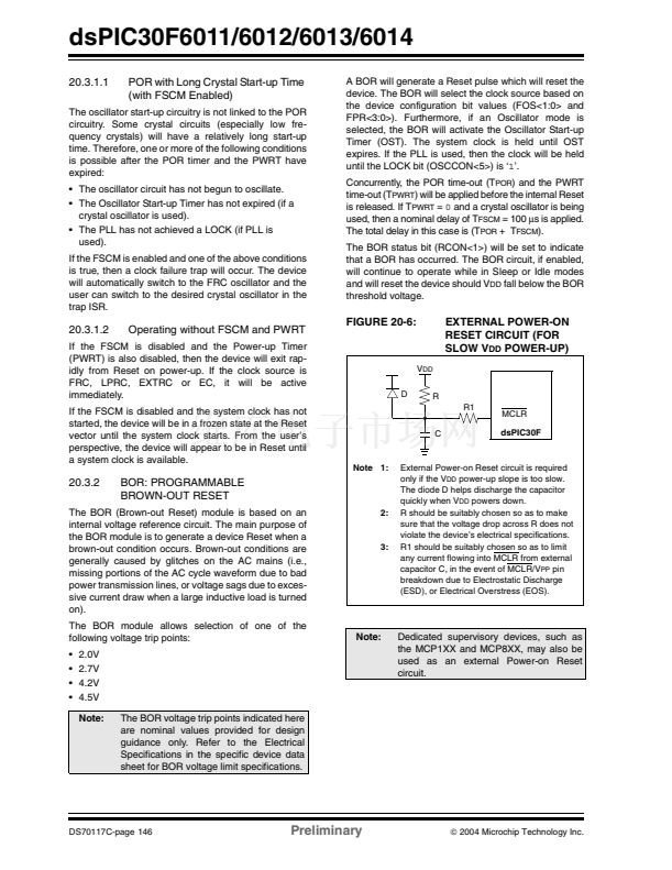
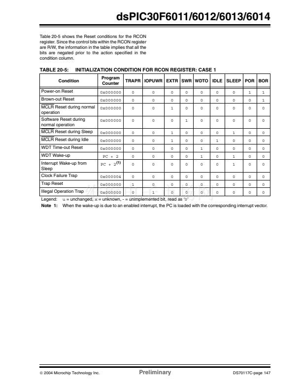
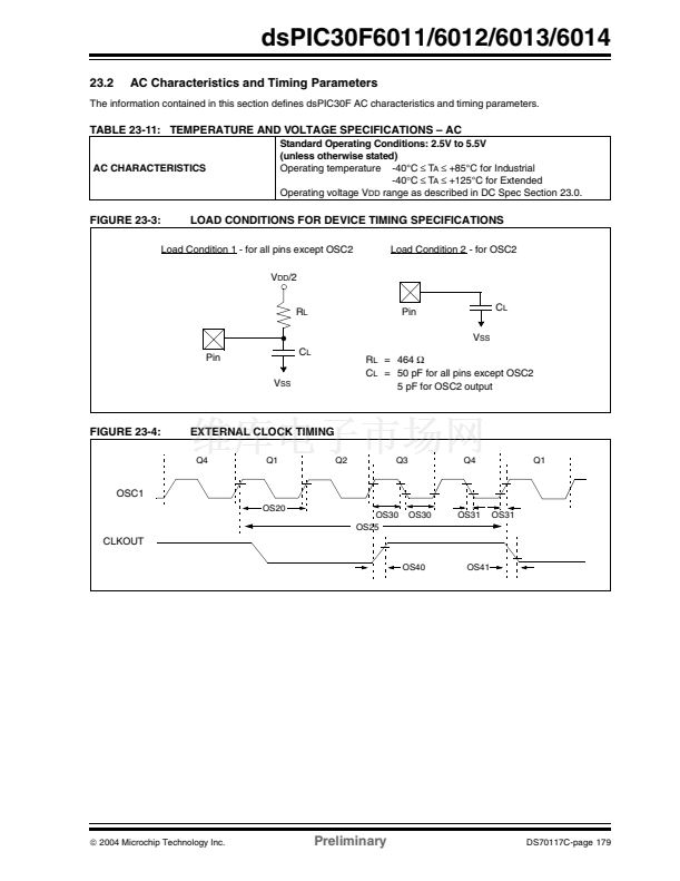
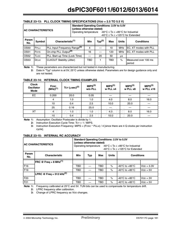
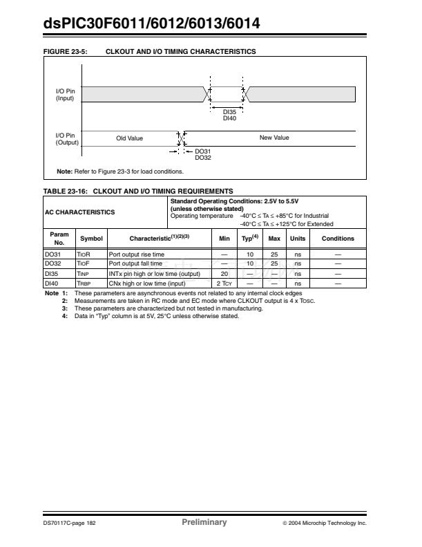
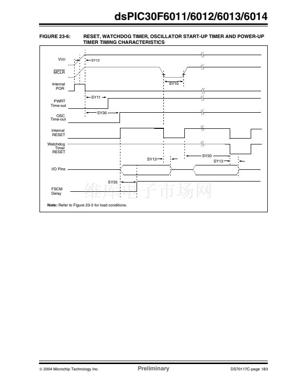
鈥?/div>
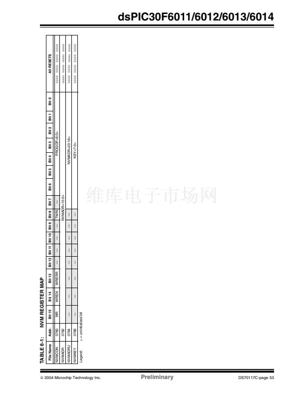
NVMCON
NVMADR
NVMADRU
NVMKEY
Control bit WR initiates write operations similar to pro-
gram Flash writes. This bit cannot be cleared, only set,
in software. They are cleared in hardware at the com-
pletion of the write operation. The inability to clear the
WR bit in software prevents the accidental or
premature termination of a write operation.
The WREN bit, when set, will allow a write operation.
On power-up, the WREN bit is clear. The WRERR bit is
set when a write operation is interrupted by a MCLR
Reset or a WDT Time-out Reset during normal opera-
tion. In these situations, following Reset, the user can
check the WRERR bit and rewrite the location. The
address register NVMADR remains unchanged.
Note:
Interrupt flag bit NVMIF in the IFS0 regis-
ter is set when write is complete. It must be
cleared in software.
The EEPROM data memory allows read and write of
single words and 16-word blocks. When interfacing to
data memory, NVMADR in conjunction with the
NVMADRU register are used to address the EEPROM
location being accessed.
TBLRDL
and
TBLWTL
instructions are used to read and write data EEPROM.
The dsPIC30F devices have up to 8 Kbytes (4K
words) of data EEPROM with an address range from
0x7FF000
to
0x7FFFFE.
A word write operation should be preceded by an erase
of the corresponding memory location(s). The write typ-
ically requires 2 ms to complete but the write time will
vary with voltage and temperature.
A program or erase operation on the data EEPROM
does not stop the instruction flow. The user is respon-
sible for waiting for the appropriate duration of time
before initiating another data EEPROM write/erase
operation. Attempting to read the data EEPROM while
a programming or erase operation is in progress results
in unspecified data.
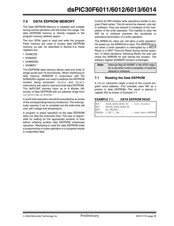
7.1
Reading the Data EEPROM
A
TBLRD
instruction reads a word at the current pro-
gram word address. This example uses W0 as a
pointer to data EEPROM. The result is placed in
register W4 as shown in Example 7-1.
EXAMPLE 7-1:
MOV
MOV
MOV
TBLRDL
DATA EEPROM READ
#LOW_ADDR_WORD,W0 ; Init Pointer
#HIGH_ADDR_WORD,W1
W1
,
TBLPAG
[ W0 ], W4
; read data EEPROM
铮?/div>
2004 Microchip Technology Inc.
Preliminary
DS70117C-page 55


 1
1
 2
2
 3
3
 4
4
 5
5
 6
6
 7
7
 8
8
 9
9
 10
10
 11
11
 12
12
 13
13
 14
14
 15
15
 16
16
 17
17
 18
18
 19
19
 20
20
 21
21
 22
22
 23
23
 24
24
 25
25
 26
26
 27
27
 28
28
 29
29
 30
30
 31
31
 32
32
 33
33
 34
34
 35
35
 36
36
 37
37
 38
38
 39
39
 40
40
 41
41
 42
42
 43
43
 44
44
 45
45
 46
46
 47
47
 48
48
 49
49
 50
50
 51
51
 52
52
 53
53
 54
54
 55
55
 56
56
 57
57
 58
58
 59
59
 60
60
 61
61
 62
62
 63
63
 64
64
 65
65
 66
66
 67
67
 68
68
 69
69
 70
70
 71
71
 72
72
 73
73
 74
74
 75
75
 76
76
 77
77
 78
78
 79
79
 80
80
 81
81
 82
82
 83
83
 84
84
 85
85
 86
86
 87
87
 88
88
 89
89
 90
90
 91
91
 92
92
 93
93
 94
94
 95
95
 96
96
 97
97
 98
98
 99
99
 100
100
 101
101
 102
102
 103
103
 104
104
 105
105
 106
106
 107
107
 108
108
 109
109
 110
110
 111
111
 112
112
 113
113
 114
114
 115
115
 116
116
 117
117
 118
118
 119
119
 120
120
 121
121
 122
122
 123
123
 124
124
 125
125
 126
126
 127
127
 128
128
 129
129
 130
130
 131
131
 132
132
 133
133
 134
134
 135
135
 136
136
 137
137
 138
138
 139
139
 140
140
 141
141
 142
142
 143
143
 144
144
 145
145
 146
146
 147
147
 148
148
 149
149
 150
150
 151
151
 152
152
 153
153
 154
154
 155
155
 156
156
 157
157
 158
158
 159
159
 160
160
 161
161
 162
162
 163
163
 164
164
 165
165
 166
166
 167
167
 168
168
 169
169
 170
170
 171
171
 172
172
 173
173
 174
174
 175
175
 176
176
 177
177
 178
178
 179
179
 180
180
 181
181
 182
182
 183
183
 184
184
 185
185
 186
186
 187
187
 188
188
 189
189
 190
190
 191
191
 192
192
 193
193
 194
194
 195
195
 196
196
 197
197
 198
198
 199
199
 200
200
 201
201
 202
202
 203
203
 204
204
 205
205
 206
206
 207
207
 208
208
 209
209
 210
210
 211
211
 212
212
 213
213
 214
214
 215
215
 216
216
 217
217
 218
218
 219
219
 220
220
 221
221
 222
222
