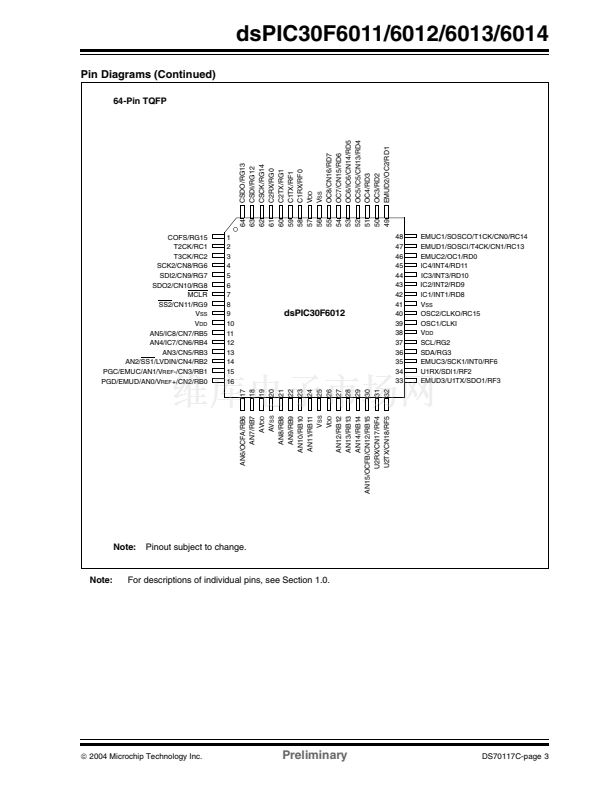
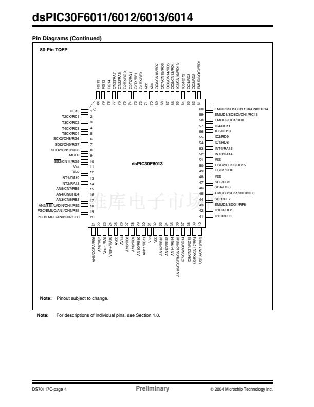
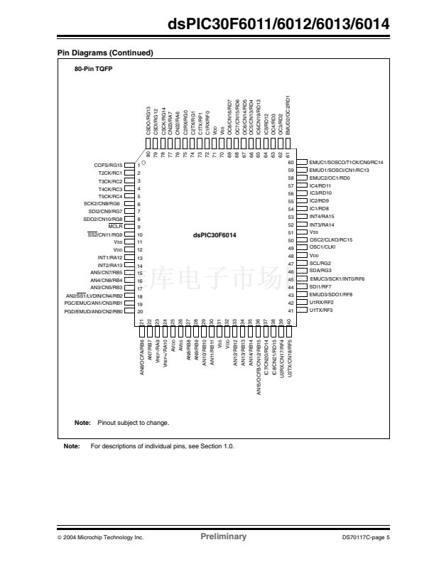
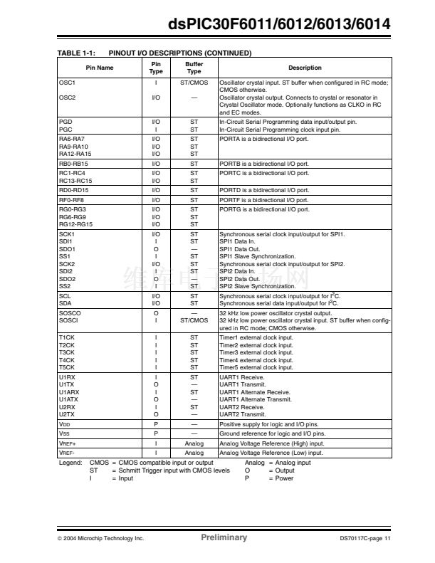
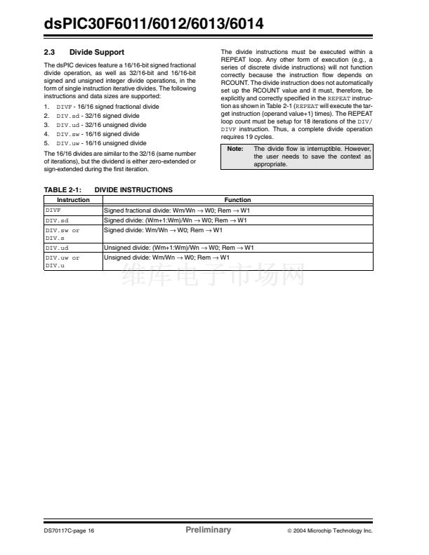
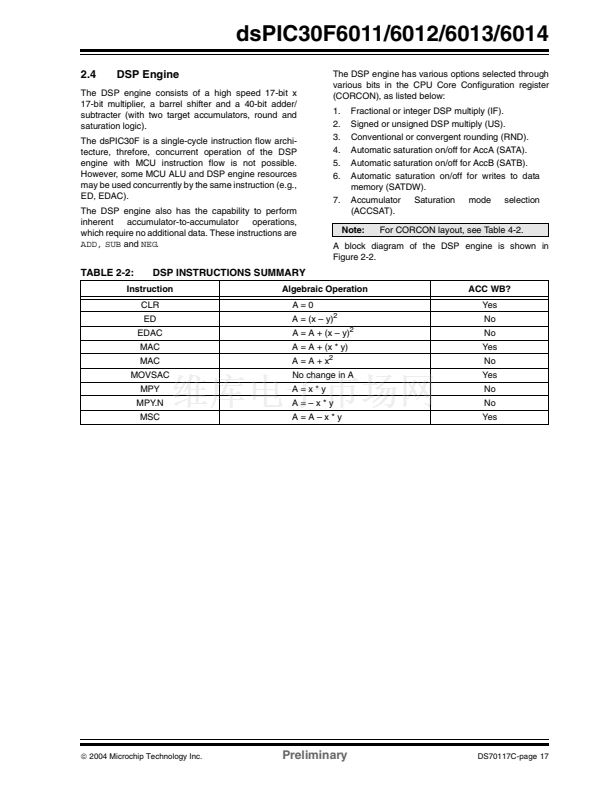
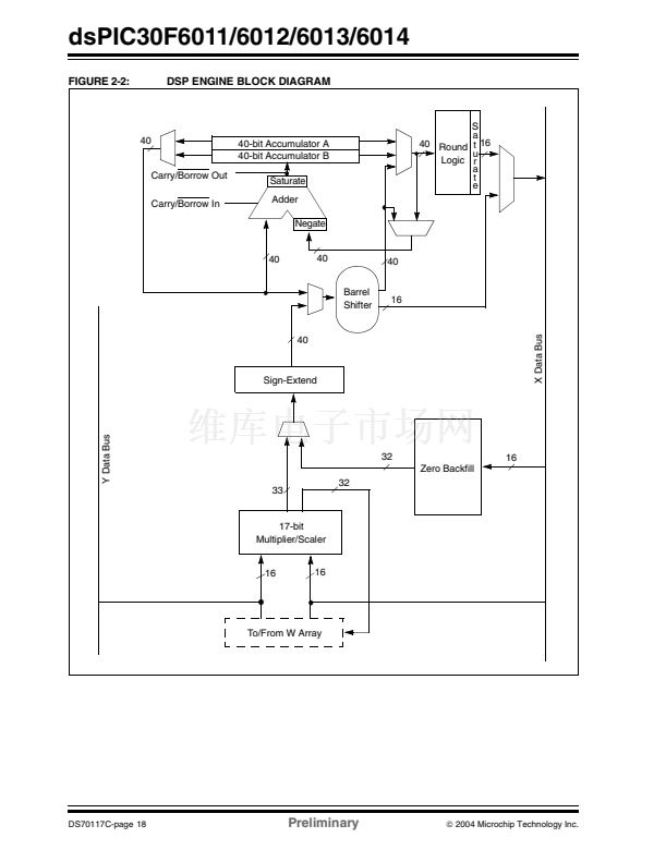
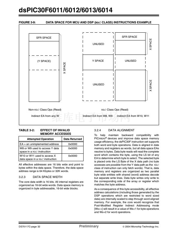
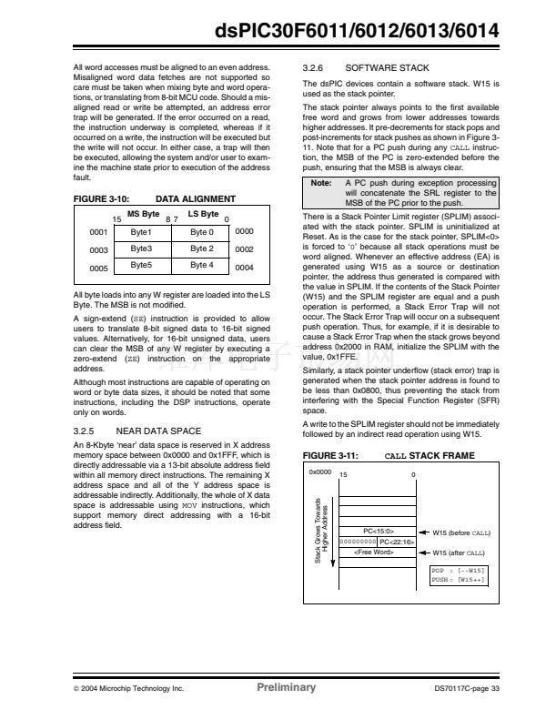
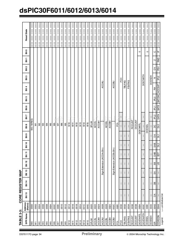
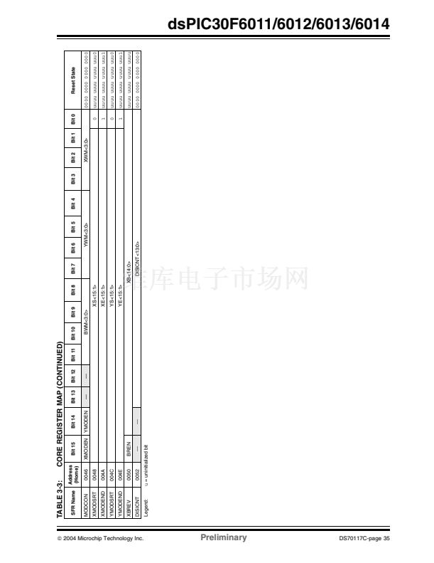
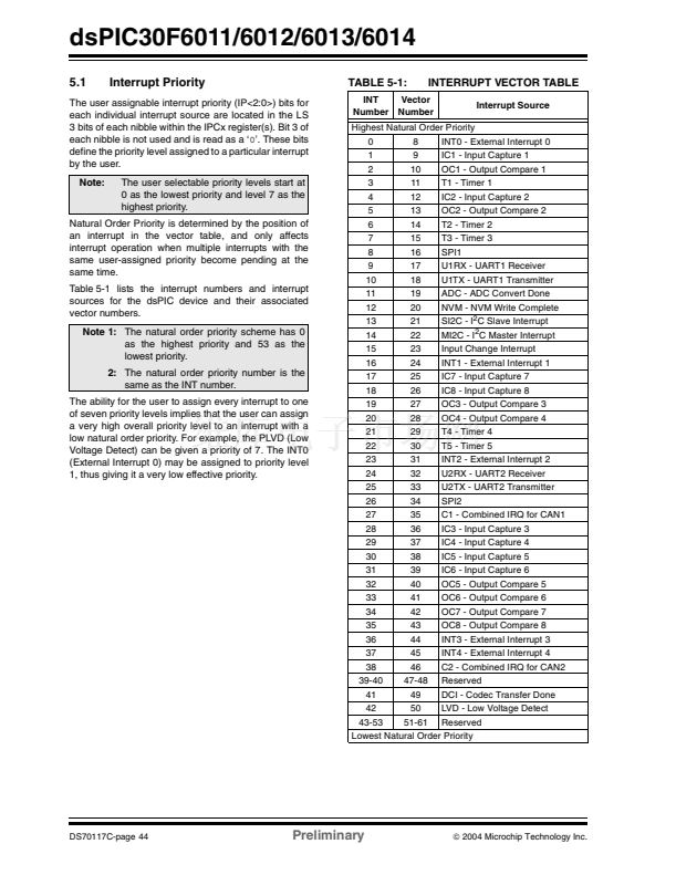
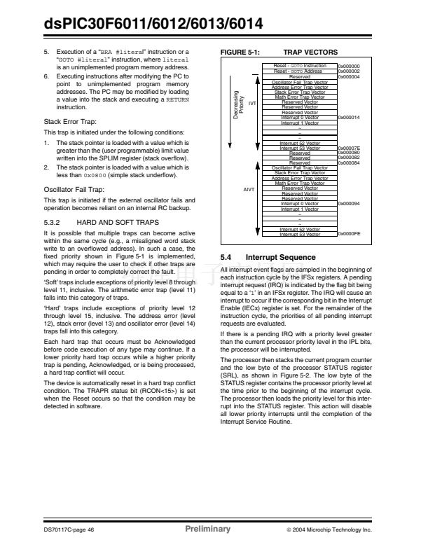
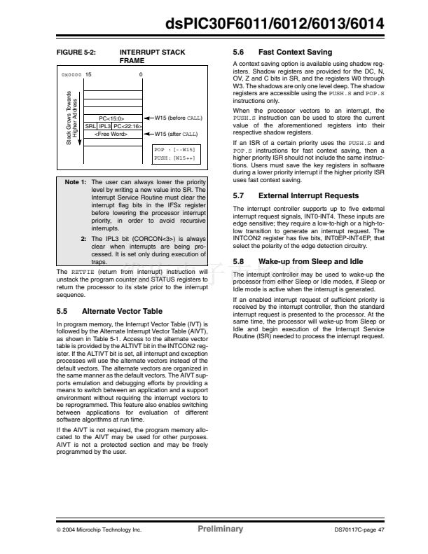
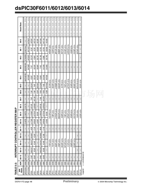
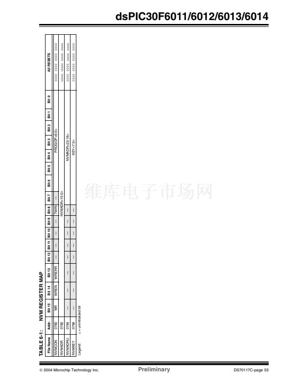
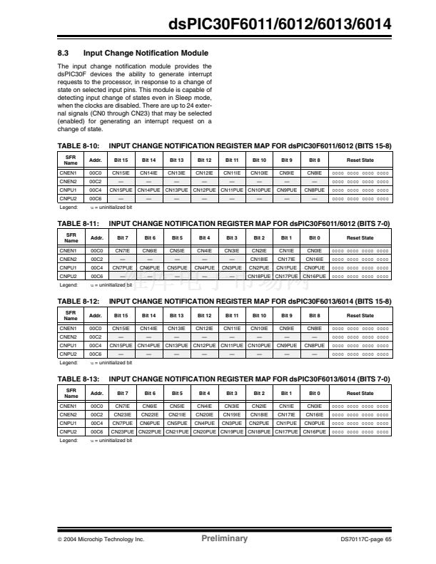
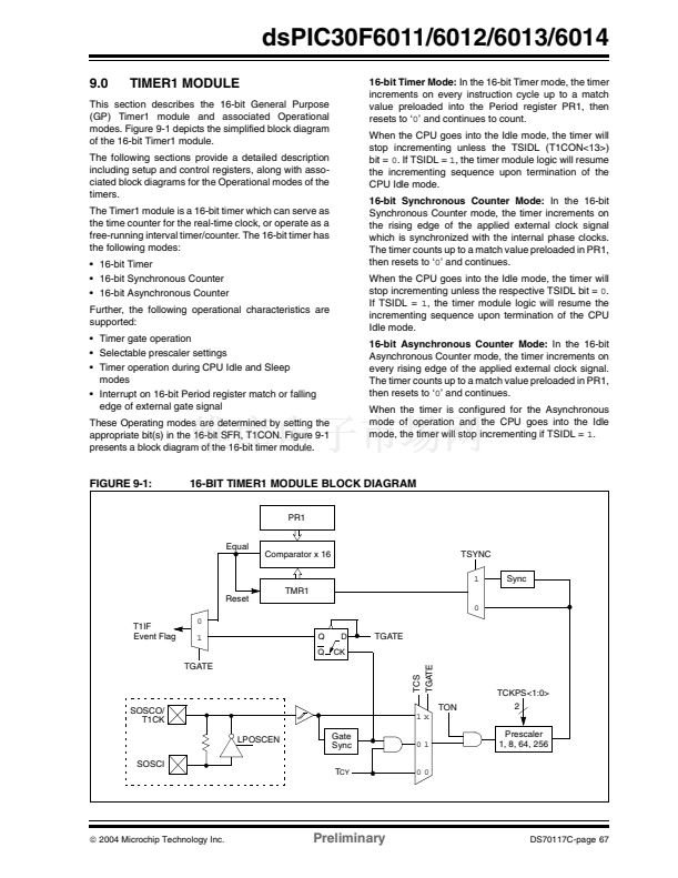
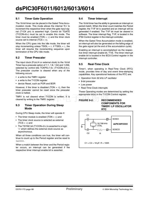
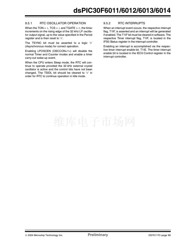
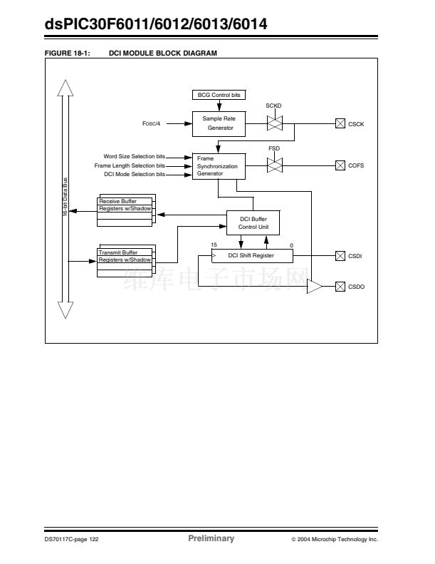
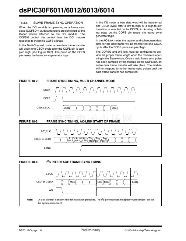
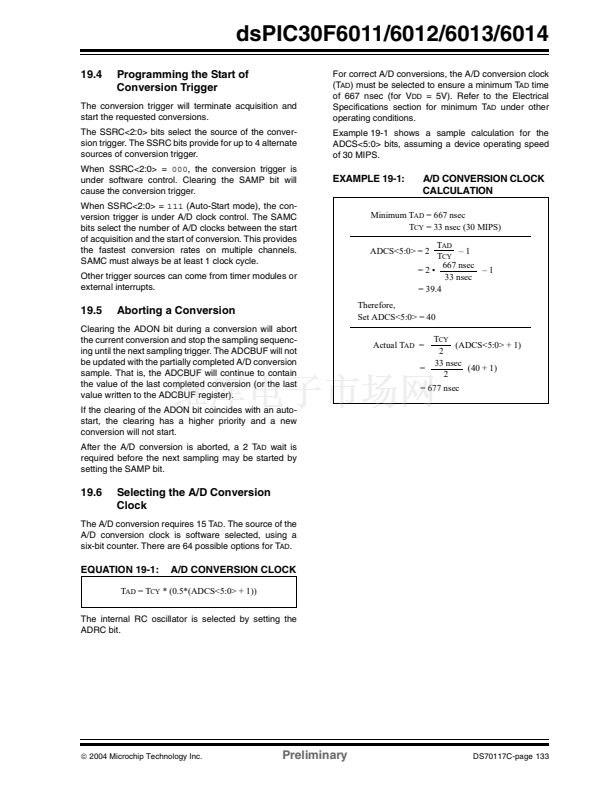
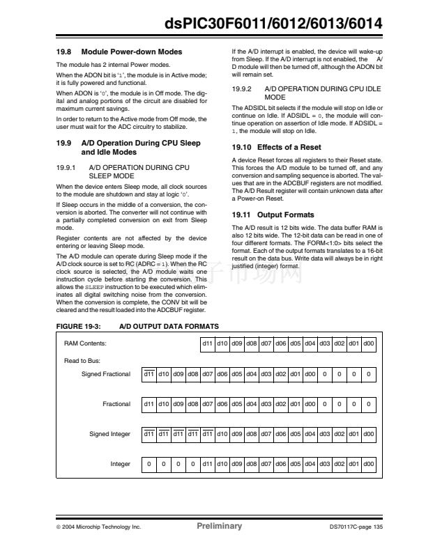
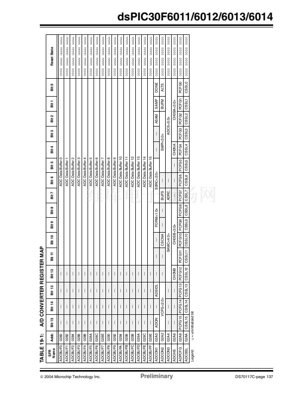
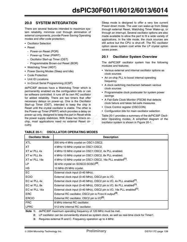
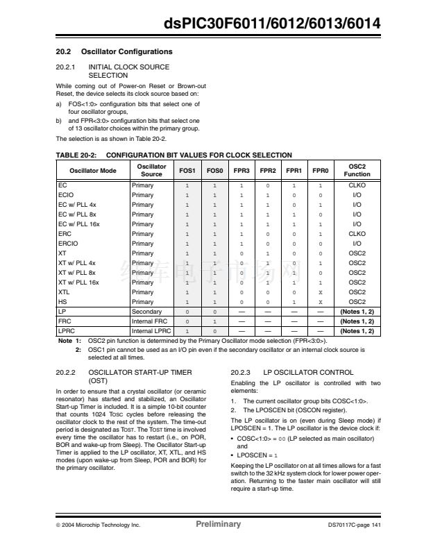
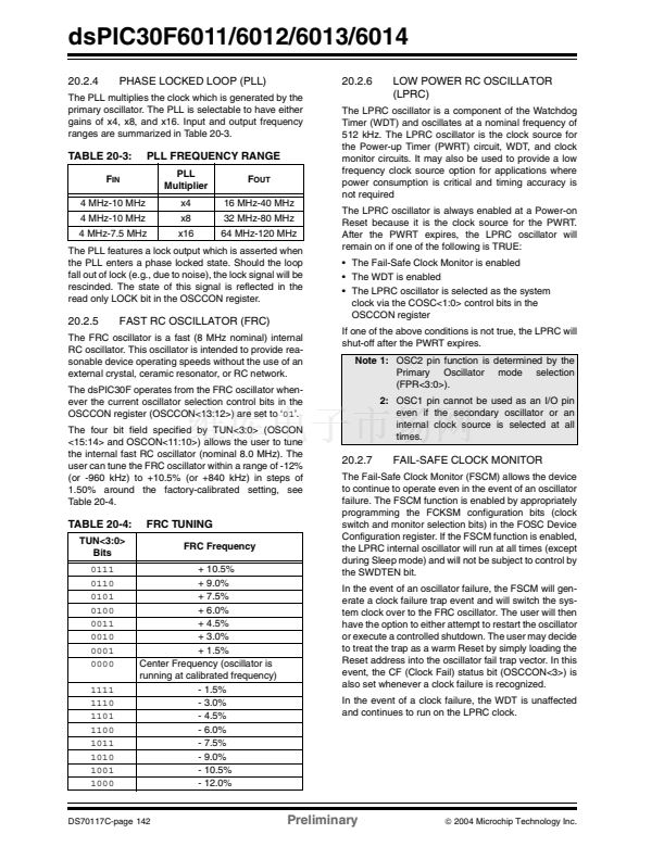
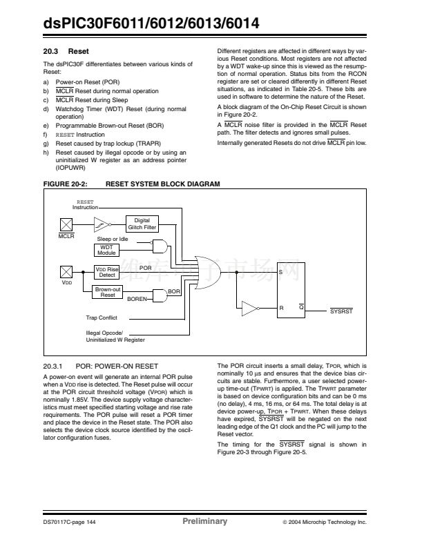
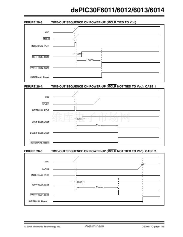
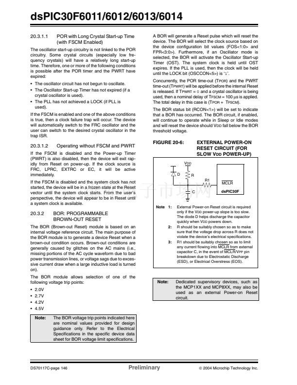
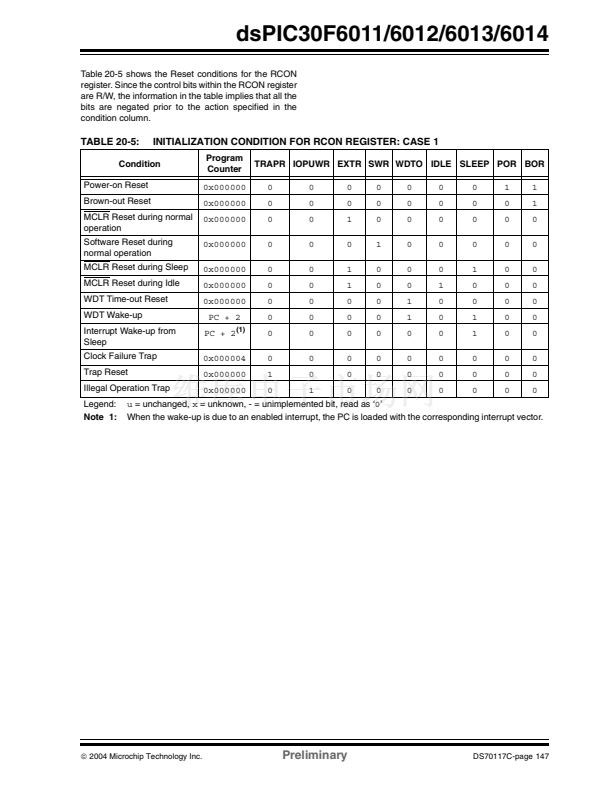
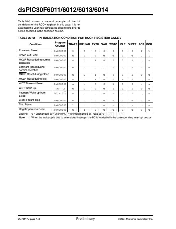
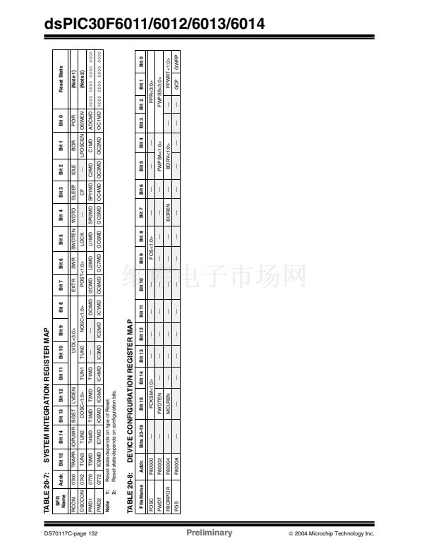
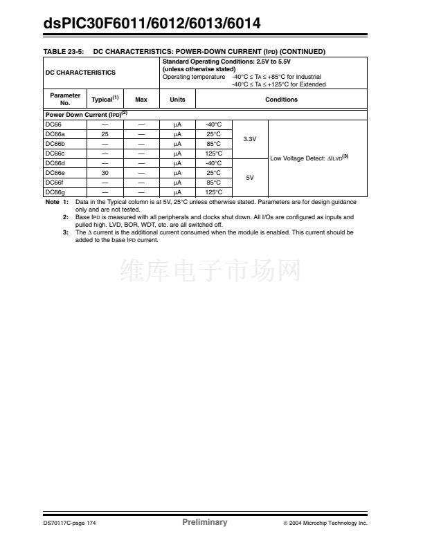
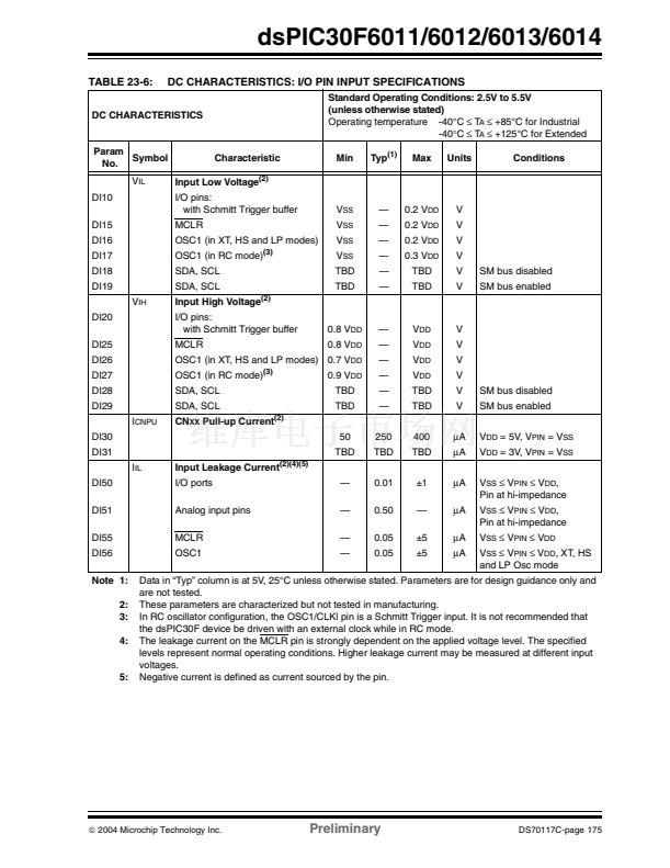
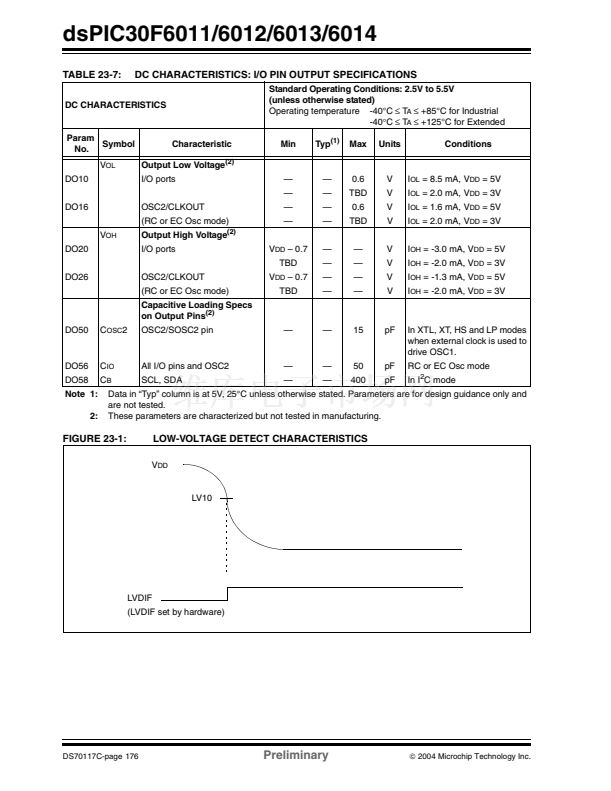
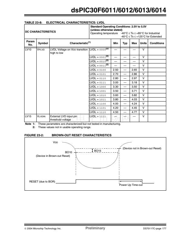
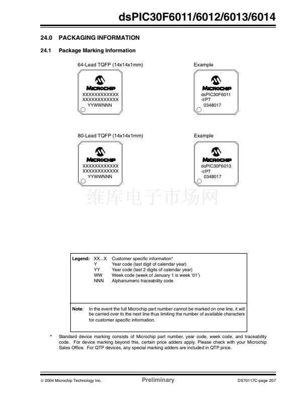
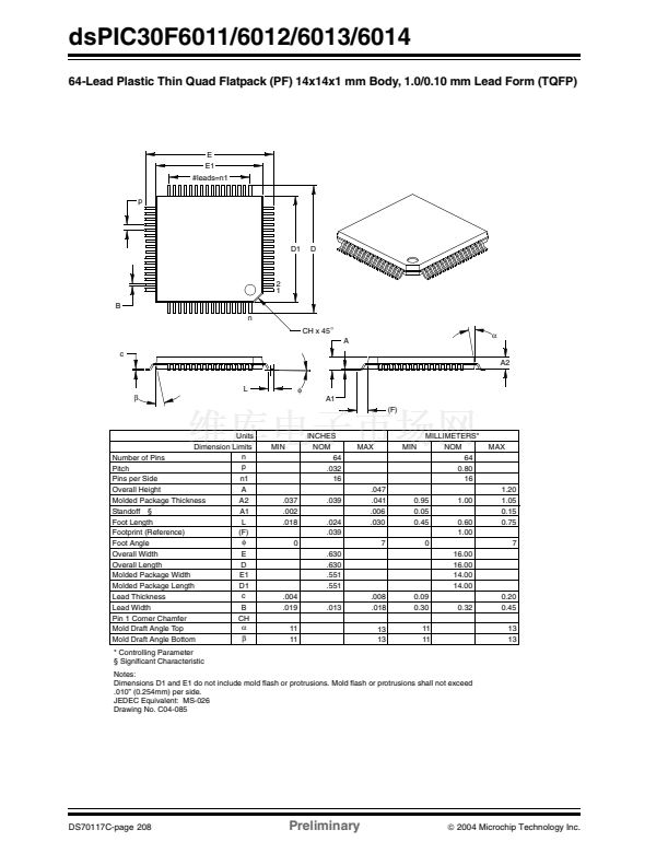
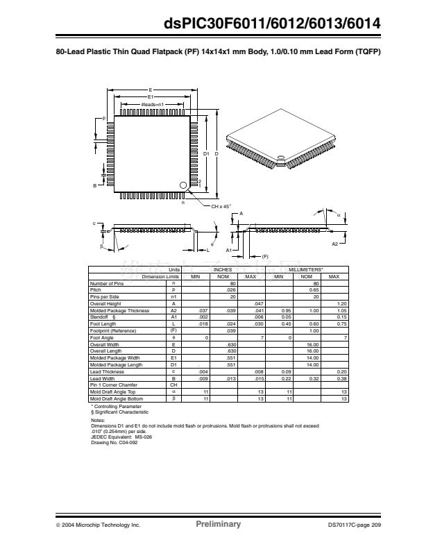
dsPIC30F6011/6012/6013/6014
15.8
Slope Control
15.12 I
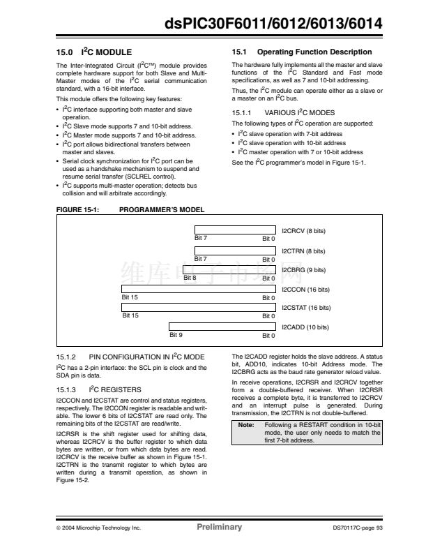
2
C Master Operation
The master device generates all of the serial clock
pulses and the Start and Stop conditions. A transfer is
ended with a Stop condition or with a Repeated Start
condition. Since the Repeated Start condition is also
the beginning of the next serial transfer, the I
2
C bus will
not be released.
In Master Transmitter mode, serial data is output
through SDA, while SCL outputs the serial clock. The
first byte transmitted contains the slave address of the
receiving device (7 bits) and the data direction bit. In
this case, the data direction bit (R_W) is logic 鈥?鈥? Serial
data is transmitted 8 bits at a time. After each byte is
transmitted, an ACK bit is received. Start and Stop con-
ditions are output to indicate the beginning and the end
of a serial transfer.
In Master Receive mode, the first byte transmitted con-
tains the slave address of the transmitting device
(7 bits) and the data direction bit. In this case, the data
direction bit (R_W) is logic 鈥?鈥? Thus, the first byte trans-
mitted is a 7-bit slave address, followed by a 鈥?鈥?to indi-
cate receive bit. Serial data is received via SDA while
SCL outputs the serial clock. Serial data is received
8 bits at a time. After each byte is received, an ACK bit
is transmitted. Start and Stop conditions indicate the
beginning and end of transmission.
The I
2
C standard requires slope control on the SDA
and SCL signals for Fast mode (400 kHz). The control
bit, DISSLW, enables the user to disable slew rate con-
trol if desired. It is necessary to disable the slew rate
control for 1 MHz mode.
15.9
IPMI Support
The control bit, IPMIEN, enables the module to support
Intelligent Peripheral Management Interface (IPMI).
When this bit is set, the module accepts and acts upon
all addresses.
15.10 General Call Address Support
The general call address can address all devices.
When this address is used, all devices should, in
theory, respond with an Acknowledgement.
The general call address is one of eight addresses
reserved for specific purposes by the I
2
C protocol. It
consists of all 鈥?鈥檚 with R_W =
0.
The general call address is recognized when the Gen-
eral Call Enable (GCEN) bit is set (I2CCON<15> =
1).
Following a Start bit detection, 8 bits are shifted into
I2CRSR and the address is compared with I2CADD,
and is also compared with the general call address
which is fixed in hardware.
If a general call address match occurs, the I2CRSR is
transferred to the I2CRCV after the eighth clock, the
RBF flag is set and on the falling edge of the ninth bit
(ACK bit), the master event interrupt flag (MI2CIF) is
set.
When the interrupt is serviced, the source for the inter-
rupt can be checked by reading the contents of the
I2CRCV to determine if the address was device
specific or a general call address.
15.12.1
I
2
C MASTER TRANSMISSION
15.11 I
2
C Master Support
As a master device, six operations are supported:
鈥?Assert a Start condition on SDA and SCL.
鈥?Assert a RESTART condition on SDA and SCL.
鈥?Write to the I2CTRN register initiating
transmission of data/address.
鈥?Generate a Stop condition on SDA and SCL.
鈥?Configure the I
2
C port to receive data.
鈥?Generate an ACK condition at the end of a
received byte of data.
Transmission of a data byte, a 7-bit address, or the sec-
ond half of a 10-bit address is accomplished by simply
writing a value to I2CTRN register. The user should
only write to I2CTRN when the module is in a WAIT
state. This action will set the Buffer Full Flag (TBF) and
allow the baud rate generator to begin counting and
start the next transmission. Each bit of address/data
will be shifted out onto the SDA pin after the falling
edge of SCL is asserted. The Transmit Status Flag,
TRSTAT (I2CSTAT<14>), indicates that a master
transmit is in progress.
15.12.2
I
2
C MASTER RECEPTION
Master mode reception is enabled by programming the
Receive Enable bit, RCEN (I2CCON<11>). The I
2
C
module must be Idle before the RCEN bit is set, other-
wise the RCEN bit will be disregarded. The baud rate
generator begins counting and on each rollover, the
state of the SCL pin ACK and data are shifted into the
I2CRSR on the rising edge of each clock.
铮?/div>
2004 Microchip Technology Inc.
Preliminary
DS70117C-page 97


 1
1
 2
2
 3
3
 4
4
 5
5
 6
6
 7
7
 8
8
 9
9
 10
10
 11
11
 12
12
 13
13
 14
14
 15
15
 16
16
 17
17
 18
18
 19
19
 20
20
 21
21
 22
22
 23
23
 24
24
 25
25
 26
26
 27
27
 28
28
 29
29
 30
30
 31
31
 32
32
 33
33
 34
34
 35
35
 36
36
 37
37
 38
38
 39
39
 40
40
 41
41
 42
42
 43
43
 44
44
 45
45
 46
46
 47
47
 48
48
 49
49
 50
50
 51
51
 52
52
 53
53
 54
54
 55
55
 56
56
 57
57
 58
58
 59
59
 60
60
 61
61
 62
62
 63
63
 64
64
 65
65
 66
66
 67
67
 68
68
 69
69
 70
70
 71
71
 72
72
 73
73
 74
74
 75
75
 76
76
 77
77
 78
78
 79
79
 80
80
 81
81
 82
82
 83
83
 84
84
 85
85
 86
86
 87
87
 88
88
 89
89
 90
90
 91
91
 92
92
 93
93
 94
94
 95
95
 96
96
 97
97
 98
98
 99
99
 100
100
 101
101
 102
102
 103
103
 104
104
 105
105
 106
106
 107
107
 108
108
 109
109
 110
110
 111
111
 112
112
 113
113
 114
114
 115
115
 116
116
 117
117
 118
118
 119
119
 120
120
 121
121
 122
122
 123
123
 124
124
 125
125
 126
126
 127
127
 128
128
 129
129
 130
130
 131
131
 132
132
 133
133
 134
134
 135
135
 136
136
 137
137
 138
138
 139
139
 140
140
 141
141
 142
142
 143
143
 144
144
 145
145
 146
146
 147
147
 148
148
 149
149
 150
150
 151
151
 152
152
 153
153
 154
154
 155
155
 156
156
 157
157
 158
158
 159
159
 160
160
 161
161
 162
162
 163
163
 164
164
 165
165
 166
166
 167
167
 168
168
 169
169
 170
170
 171
171
 172
172
 173
173
 174
174
 175
175
 176
176
 177
177
 178
178
 179
179
 180
180
 181
181
 182
182
 183
183
 184
184
 185
185
 186
186
 187
187
 188
188
 189
189
 190
190
 191
191
 192
192
 193
193
 194
194
 195
195
 196
196
 197
197
 198
198
 199
199
 200
200
 201
201
 202
202
 203
203
 204
204
 205
205
 206
206
 207
207
 208
208
 209
209
 210
210
 211
211
 212
212
 213
213
 214
214
 215
215
 216
216
 217
217
 218
218
 219
219
 220
220
 221
221
 222
222
