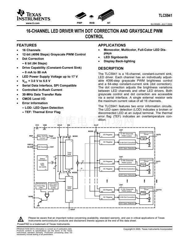
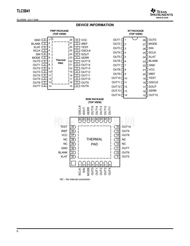
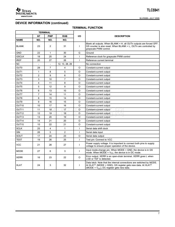
TLC5941
www.ti.com
SLVS589 鈥?JULY 2005
POWER DISSIPATION CALCULATION
The device power dissipation needs to be below the power dissipation rate of the device package to ensure
correct operation.
Equation 2
calculates the power dissipation of device:
P
D
+
V
CC
I
CC
)
V
OUT
I
MAX
N
DCn
63
d
PWM
(2)
where:
V
CC
: device supply voltage
I
CC
: device supply current
V
OUT
: TLC5941 OUTn voltage when driving LED current
I
MAX
: LED current adjusted by R
(IREF)
Resistor
DC
n
: maximum dot correction value for OUTn
N: number of OUTn driving LED at the same time
d
PWM
: duty cycle defined by BLANK pin or GS PWM value
OPERATING MODES
Table 3
shows the available operating modes. The TLC5941 GS operating mode (see
Figure 10)
and shift
register values are not defined after power up. One solution to solve this is to set dot correction data after
TLC5941 power up and switch back to GS PWM mode. The other solution is to overflow the input shift register
with 193 bits of dummy data and latch it while TLC5941 is in GS PWM mode.
Table 3. MODE Signal Truth Table
MODE
LOW
HIGH
INPUT SHIFT REGISTER
192 bit
96 bit
OPERATING MODE
Grayscale PWM Mode
Dot Correction Data Input Mode
SETTING DOT CORRECTION
The TLC5941 has the capability to fine-adjust the output current of each channel (OUT0 to OUT15)
independently. This is also called dot correction. This feature is used to adjust the brightness deviations of LEDs
connected to the output channels OUT0 to OUT15. Each of the 16 channels can be programmed with a 6-bit
word. The channel output can be adjusted in 64 steps from 0% to 100% of the maximum output current I
max
.
Equation 3
determines the output current for each output n:
I
+
I max DCn
OUTn
63
(3)
where:
I
max
= the maximum programmable output current for each output.
DCn = the programmed dot correction value for output n (DCn = 0 to 63).
n = 0 to 15
Dot correction data are entered for all channels at the same time. The complete dot correction data format
consists of 16 x 6-bit words, which forms a 96-bit wide serial data packet. The channel data is put one after
another. All data is clocked in with MSB first.
Figure 7
shows the DC data format.
13


 1
1
 2
2
 3
3
 4
4
 5
5
 6
6
 7
7
 8
8
 9
9
 10
10
 11
11
 12
12
 13
13
 14
14
 15
15
 16
16
 17
17
 18
18
 19
19
 20
20
 21
21
 22
22
 23
23
