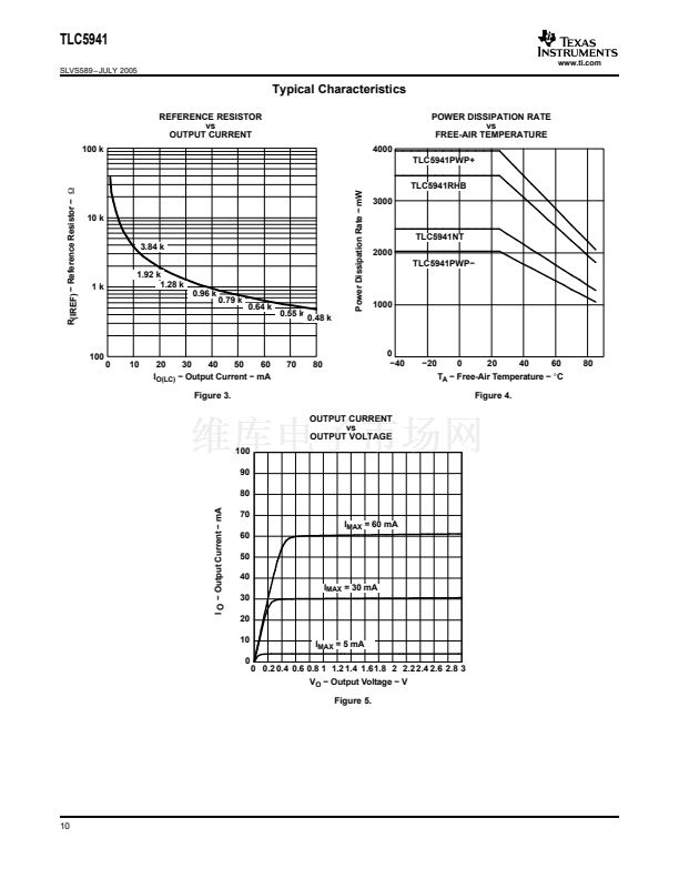
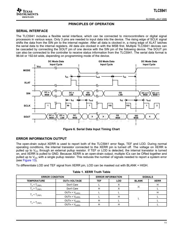
TLC5941
www.ti.com
SLVS589 鈥?JULY 2005
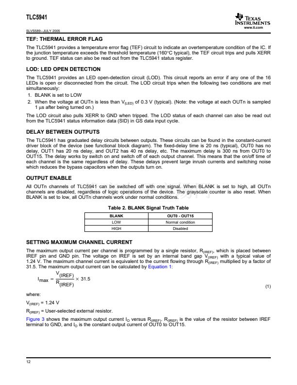
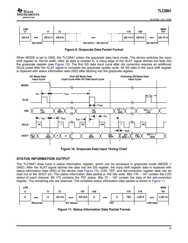
LSB
0
DC 0.0
DC OUT0
5
DC 0.5
6
DC 1.0
DC OUT2 鈭?DC OUT14
79
DC 14.5
90
DC 15.0
DC OUT15
MSB
95
DC 15.5
Figure 7. Dot Correction Data Packet Format
To input data into the dot correction register, MODE must be set to V
CC
. The internal input shift register is then
set to 96-bit width. After all serial data are clocked in, a rising edge of XLAT is used to latch the data into the dot
correction register.
Figure 8
shows the dc data input timing chart.
DC Mode Data
Input Cycle n
V
CC
MODE
SIN
DC n鈭?
LSB
DC n
MSB
DC n
MSB鈭?
DC n
MSB鈭?
DC n
LSB+1
DC n
LSB
DC n+1
MSB
DC n+1
MSB鈭?
DC Mode Data
Input Cycle n+1
t
wh0
SCLK
1
2
t
wl0
SOUT
DC n鈭?
MSB
DC n鈭?
MSB鈭?
DC n鈭?
MSB鈭?
DC n鈭?
LSB+1
DC n鈭?
LSB
DC n
MSB
DC n
MSB鈭?
DC n
MSB鈭?
3
95
96
1
2
t
su1
XLAT
t
wh2
t
h1
Figure 8. Dot Correction Data Input Timing Chart
SETTING GRAYSCALE
The TLC5941 can adjust the brightness of each channel OUTn using a PWM control scheme. The use of 12 bits
per channel results in 4096 different brightness steps, from 0% to 100% brightness.
Equation 4
determines the
brightness level for each output n:
Brightness in %
+
GSn
100
4095
(4)
where:
GSn = the programmed grayscale value for output n (GSn = 0 to 4095)
n = 0 to 15
Grayscale data for all OUTn
The input shift register enters grayscale data into the grayscale register for all channels simultaneously. The
complete grayscale data format consists of 16 x 12 bit words, which forms a 192-bit wide data packet (see
Figure 9).
The data packet must be clocked in with the MSB first.
14


 1
1
 2
2
 3
3
 4
4
 5
5
 6
6
 7
7
 8
8
 9
9
 10
10
 11
11
 12
12
 13
13
 14
14
 15
15
 16
16
 17
17
 18
18
 19
19
 20
20
 21
21
 22
22
 23
23
