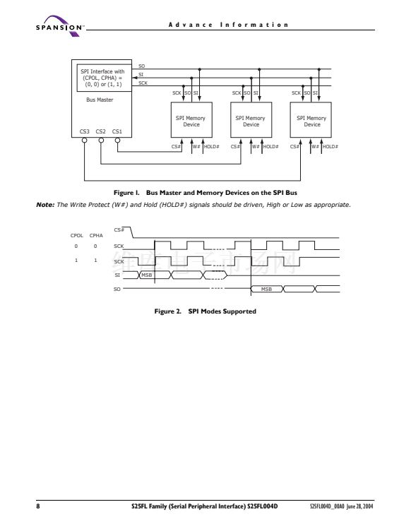
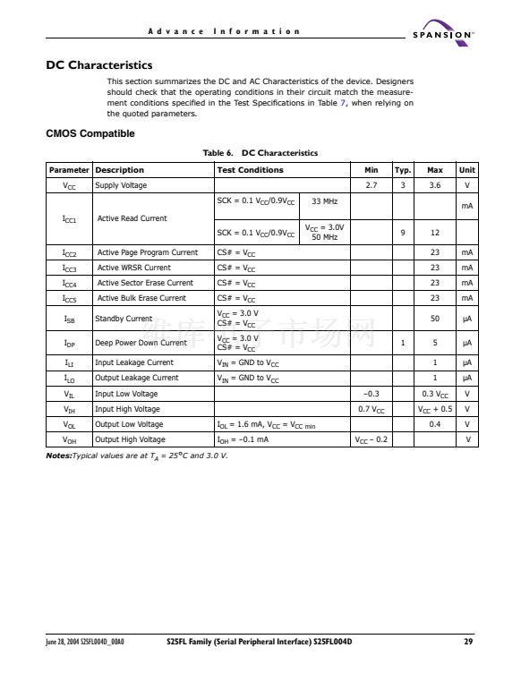
A d v a n c e
I n f o r m a t i o n
been set. The Bulk Erase (BE) instruction is executed if, and only if, all Block Pro-
tect (BP2, BP1, BP0) bits are 0.
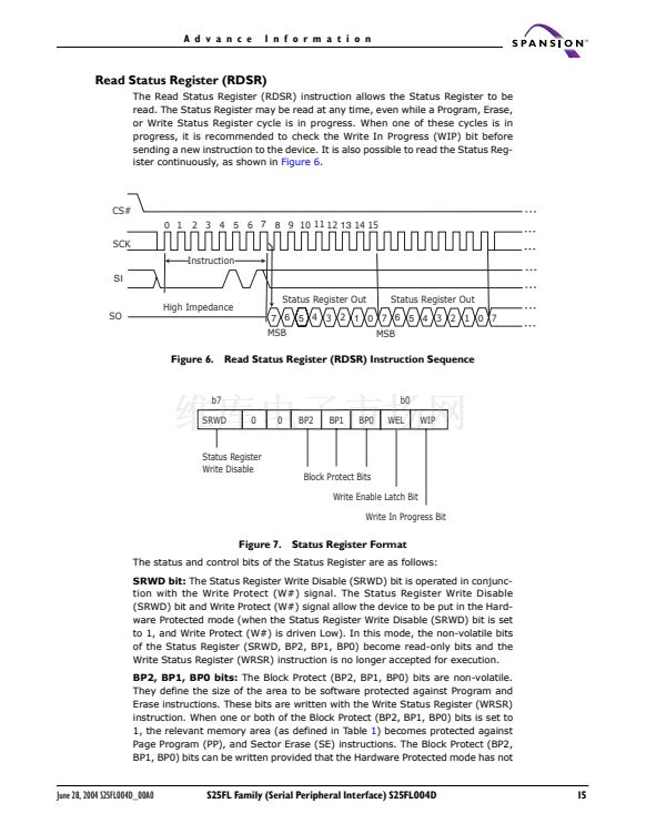
WEL bit:
The Write Enable Latch (WEL) bit indicates the status of the internal
Write Enable Latch. When set to 1, the internal Write Enable Latch is set; when
set to 0, the internal Write Enable Latch is reset and no Write Status Register, Pro-
gram or Erase instruction is accepted.
WIP bit:
The Write In Progress (WIP) bit indicates whether the memory is busy
with a Write Status Register, Program or Erase cycle. This bit is a read only bit
and is read by executing a RDSR instruction. If this bit is 1, such a cycle is in
progress, if it is 0, no such cycle is in progress.
Write Status Register (WRSR)
The Write Status Register (WRSR) instruction allows new values to be written to
the Status Register. Before it can be accepted, a Write Enable (WREN) instruction
must previously have been executed. After the Write Enable (WREN) instruction
has been decoded and executed, the device sets the Write Enable Latch (WEL).
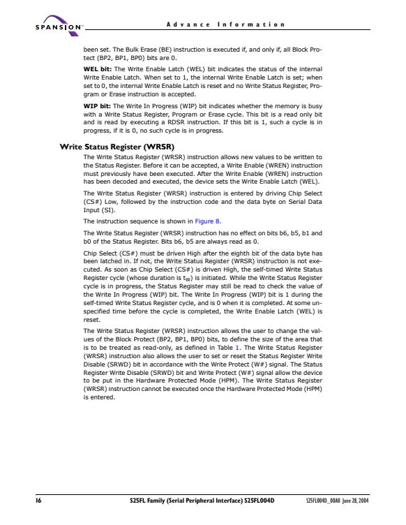
The Write Status Register (WRSR) instruction is entered by driving Chip Select
(CS#) Low, followed by the instruction code and the data byte on Serial Data
Input (SI).
The instruction sequence is shown in
Figure 8.
The Write Status Register (WRSR) instruction has no effect on bits b6, b5, b1 and
b0 of the Status Register. Bits b6, b5 are always read as 0.
Chip Select (CS#) must be driven High after the eighth bit of the data byte has
been latched in. If not, the Write Status Register (WRSR) instruction is not exe-
cuted. As soon as Chip Select (CS#) is driven High, the self-timed Write Status
Register cycle (whose duration is t
W
) is initiated. While the Write Status Register
cycle is in progress, the Status Register may still be read to check the value of
the Write In Progress (WIP) bit. The Write In Progress (WIP) bit is 1 during the
self-timed Write Status Register cycle, and is 0 when it is completed. At some un-
specified time before the cycle is completed, the Write Enable Latch (WEL) is
reset.
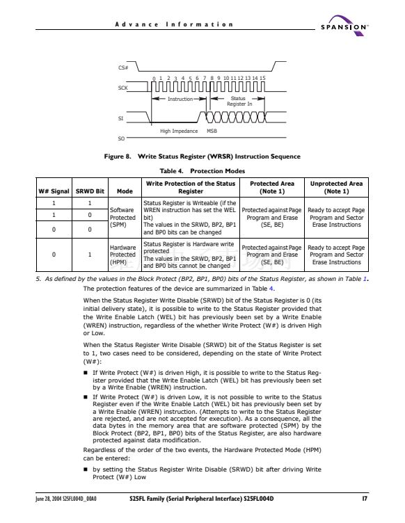
The Write Status Register (WRSR) instruction allows the user to change the val-
ues of the Block Protect (BP2, BP1, BP0) bits, to define the size of the area that
is to be treated as read-only, as defined in Table
1.
The Write Status Register
(WRSR) instruction also allows the user to set or reset the Status Register Write
Disable (SRWD) bit in accordance with the Write Protect (W#) signal. The Status
Register Write Disable (SRWD) bit and Write Protect (W#) signal allow the device
to be put in the Hardware Protected Mode (HPM). The Write Status Register
(WRSR) instruction cannot be executed once the Hardware Protected Mode (HPM)
is entered.
16
S25FL Family (Serial Peripheral Interface) S25FL004D
S25FL004D_00A0 June 28, 2004


 1
1
 2
2
 3
3
 4
4
 5
5
 6
6
 7
7
 8
8
 9
9
 10
10
 11
11
 12
12
 13
13
 14
14
 15
15
 16
16
 17
17
 18
18
 19
19
 20
20
 21
21
 22
22
 23
23
 24
24
 25
25
 26
26
 27
27
 28
28
 29
29
 30
30
 31
31
 32
32
 33
33
 34
34
 35
35
 36
36
