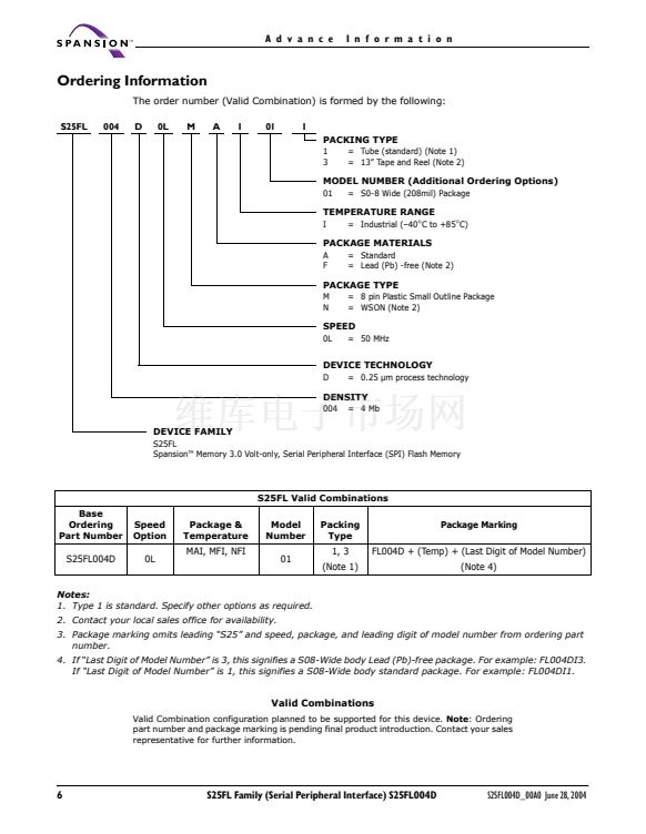
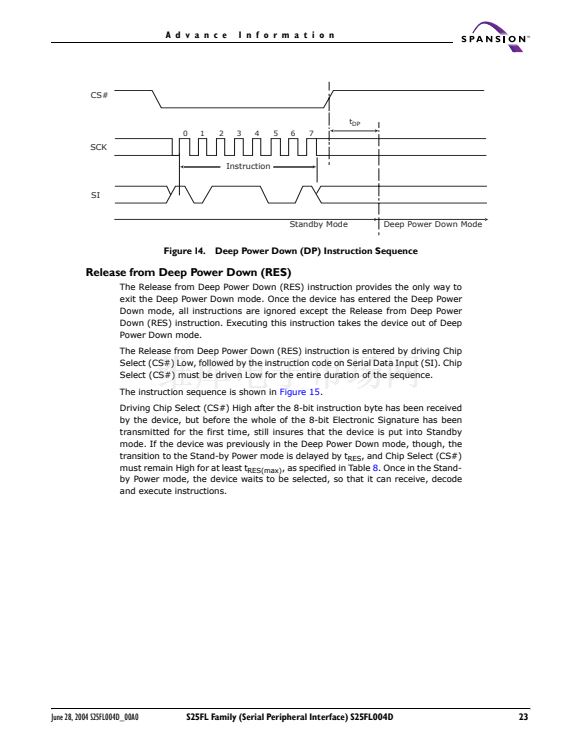
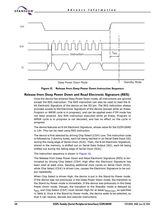
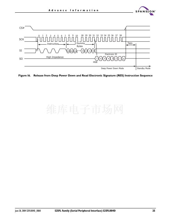
A d v a n c e
I n f o r m a t i o n
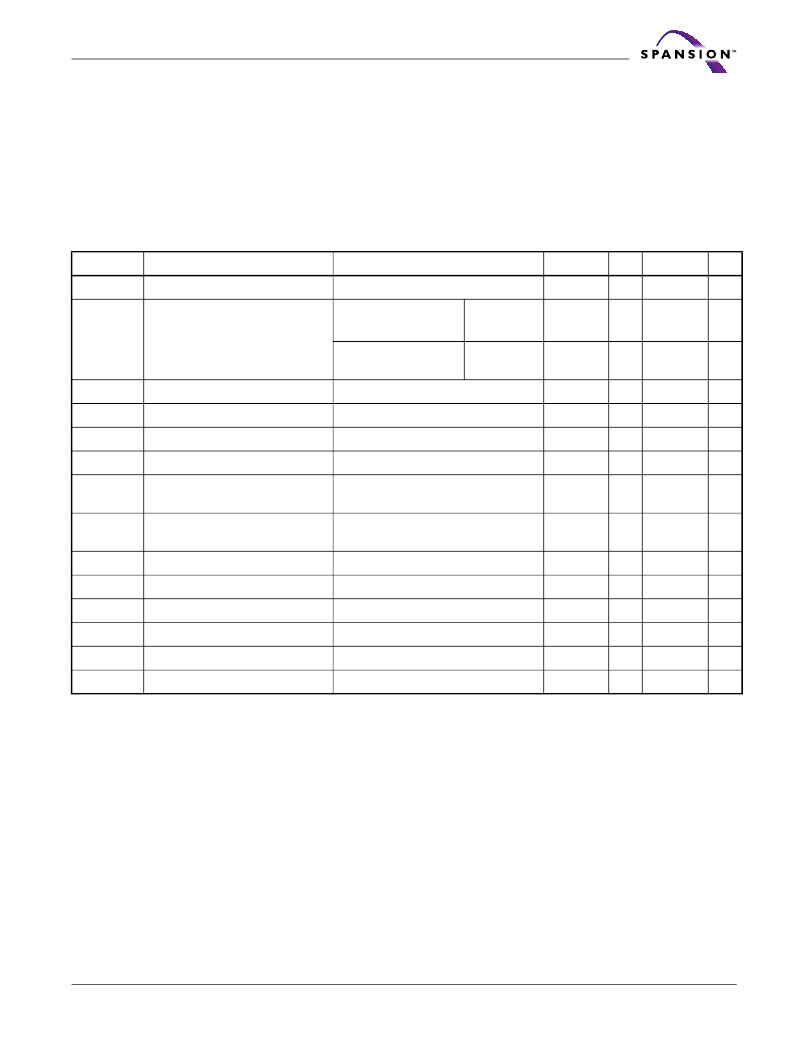
DC Characteristics
This section summarizes the DC and AC Characteristics of the device. Designers
should check that the operating conditions in their circuit match the measure-
ment conditions specified in the Test Specifications in Table
7,
when relying on
the quoted parameters.
CMOS Compatible
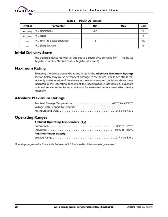
Table 6.
Parameter Description
V
CC
Supply Voltage
SCK = 0.1 V
CC
/0.9V
CC
I
CC1
Active Read Current
SCK = 0.1 V
CC
/0.9V
CC
I
CC2
I
CC3
I
CC4
I
CC5
I
SB
I
DP
I
LI
I
LO
V
IL
V
IH
V
OL
V
OH
Active Page Program Current
Active WRSR Current
Active Sector Erase Current
Active Bulk Erase Current
Standby Current
Deep Power Down Current
Input Leakage Current
Output Leakage Current
Input Low Voltage
Input High Voltage
Output Low Voltage
Output High Voltage
I
OL
= 1.6 mA, V
CC
= V
CC min
I
OH
= 鈥?.1 mA
V
CC
鈥?0.2
CS# = V
CC
CS# = V
CC
CS# = V
CC
CS# = V
CC
V
CC
= 3.0 V
CS# = V
CC
V
CC
= 3.0 V
CS# = V
CC
V
IN
= GND to V
CC
V
IN
= GND to V
CC
鈥?.3
0.7 V
CC
1
33 MHz
V
CC
= 3.0V
50 MHz
DC Characteristics
Min
2.7
Typ.
3
Max
3.6
Unit
V
mA
9
12
23
23
23
23
50
5
1
1
0.3 V
CC
V
CC
+ 0.5
0.4
mA
mA
mA
mA
碌A
碌A
碌A
碌A
V
V
V
V
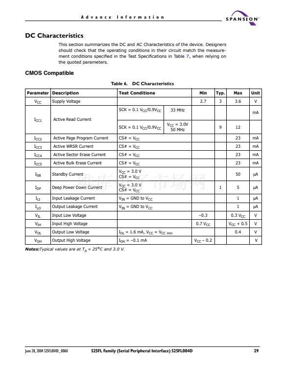
Test Conditions
Notes:Typical
values are at T
A
= 25
掳
C and 3.0 V.
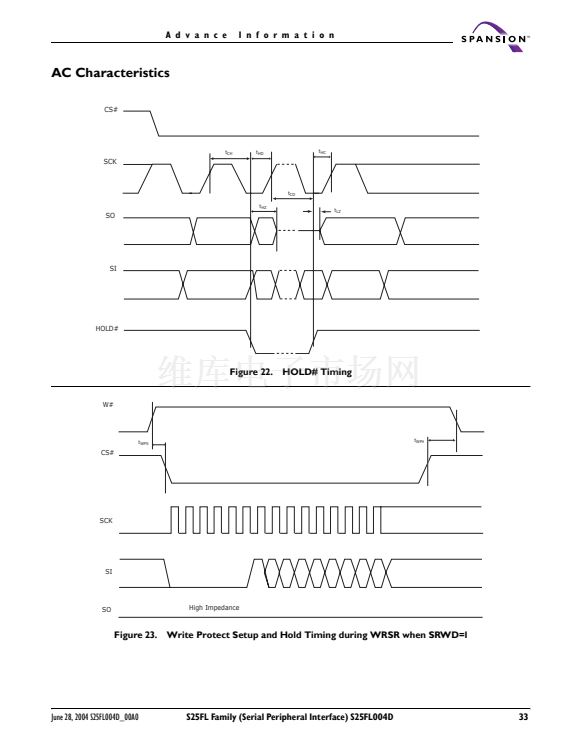
June 28, 2004 S25FL004D_00A0
S25FL Family (Serial Peripheral Interface) S25FL004D
29


 1
1
 2
2
 3
3
 4
4
 5
5
 6
6
 7
7
 8
8
 9
9
 10
10
 11
11
 12
12
 13
13
 14
14
 15
15
 16
16
 17
17
 18
18
 19
19
 20
20
 21
21
 22
22
 23
23
 24
24
 25
25
 26
26
 27
27
 28
28
 29
29
 30
30
 31
31
 32
32
 33
33
 34
34
 35
35
 36
36
