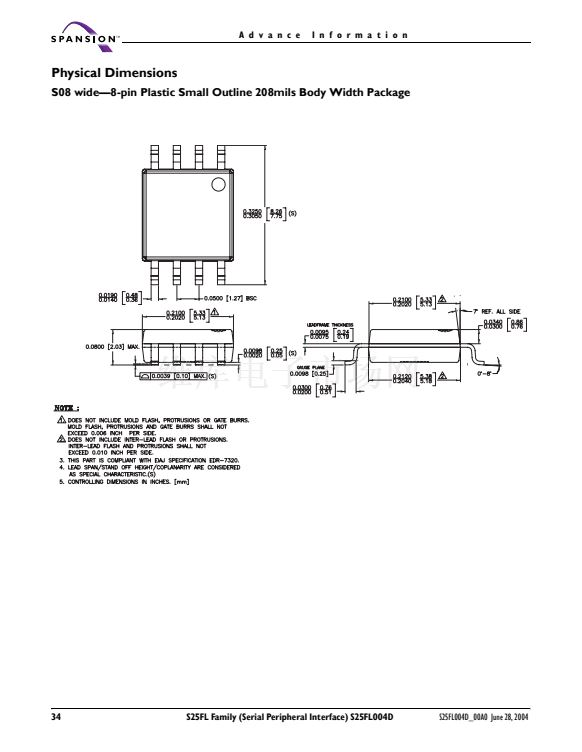
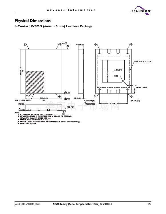
A d v a n c e
I n f o r m a t i o n
Operating Features
All data into and out of the device is shifted in 8-bit chunks.
Page Programming
To program one data byte, two instructions are required: Write Enable (WREN),
which is one byte, and a Page Program (PP) sequence, which consists of four
bytes plus data. This is followed by the internal Program cycle. To spread this
overhead, the Page Program (PP) instruction allows up to 256 bytes to be pro-
grammed at a time (changing bits from 1 to 0), provided that they lie in
consecutive addresses on the same page of memory.
Sector Erase, or Bulk Erase
The Page Program (PP) instruction allows bits to be programmed from 1 to 0. Be-
fore this can be applied, the bytes of the memory need to be first erased to all
1鈥檚 (FFh) before any programming. This can be achieved in two ways: 1) a sector
at a time using the Sector Erase (SE) instruction, or 2) throughout the entire
memory, using the Bulk Erase (BE) instruction.
Polling During a Write, Program, or Erase Cycle
A further improvement in the time to Write Status Register (WRSR), Program (PP)
or Erase (SE or BE) can be achieved by not waiting for the worst-case delay. The
Write in Progress (WIP) bit is provided in the Status Register so that the applica-
tion program can monitor its value, polling it to establish when the previous Write
cycle, Program cycle, or Erase cycle is complete.
Active Power and Standby Power Modes
When Chip Select (CS#) is Low, the device is enabled, and in the Active Power
mode. When Chip Select (CS#) is High, the device is disabled, but could remain
in the Active Power mode until all internal cycles have completed (Program,
Erase, Write Status Register). The device then goes into the Standby Power
mode. The device consumption drops to I
SB
. This can be used as an extra Deep
Power Down on mechanism, when the device is not in active use, to protect the
device from inadvertent Write, Program, or Erase instructions.
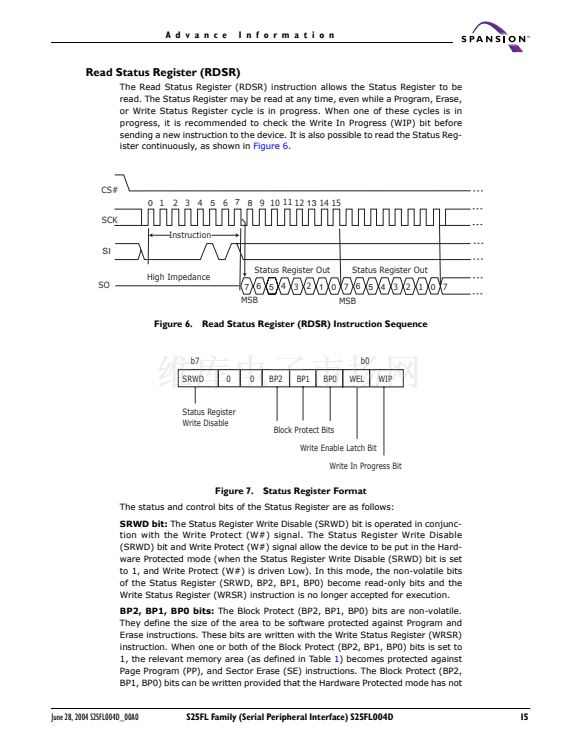
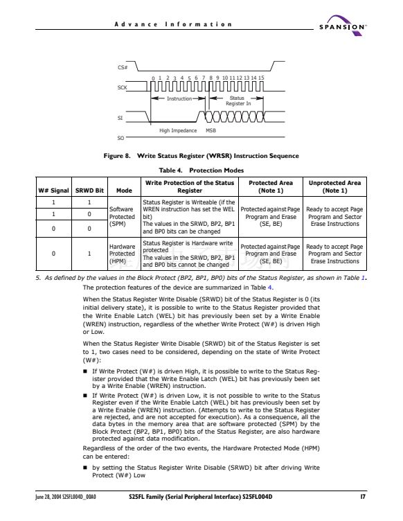
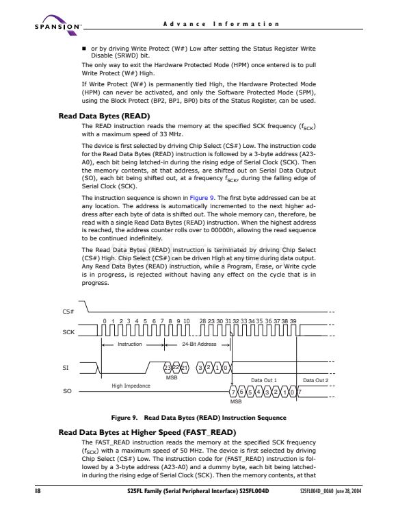
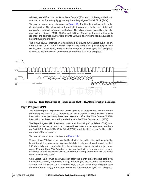
Status Register
The Status Register contains a number of status and control bits, as shown in
Fig-
ure 7,
that can be read or set (as appropriate) by specific instructions
WIP bit:
The Write In Progress (WIP) bit indicates whether the memory is
busy with a Write Status Register, Program or Erase cycle.
WEL bit:
The Write Enable Latch (WEL) bit indicates the status of the internal
Write Enable Latch.
BP2, BP1, BP0 bits:
The Block Protect (BP2, BP1, BP0) bits are non-volatile.
They define the size of the area to be software protected against Program and
Erase instructions.
SRWD bit:
The Status Register Write Disable (SRWD) bit is operated in con-
junction with the Write Protect (W#) signal. The Status Register Write Disable
(SRWD) bit and Write Protect (W#) signal allow the device to be put in the
Hardware Protected mode. In this mode, the non-volatile bits of the Status
Register (SRWD, BP2, BP1, BP0) become read-only bits.
June 28, 2004 S25FL004D_00A0
S25FL Family (Serial Peripheral Interface) S25FL004D
9


 1
1
 2
2
 3
3
 4
4
 5
5
 6
6
 7
7
 8
8
 9
9
 10
10
 11
11
 12
12
 13
13
 14
14
 15
15
 16
16
 17
17
 18
18
 19
19
 20
20
 21
21
 22
22
 23
23
 24
24
 25
25
 26
26
 27
27
 28
28
 29
29
 30
30
 31
31
 32
32
 33
33
 34
34
 35
35
 36
36
