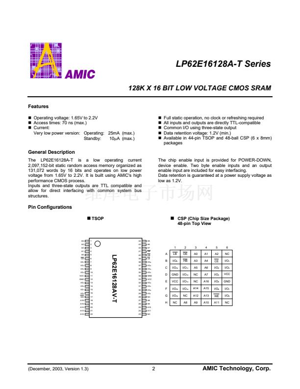
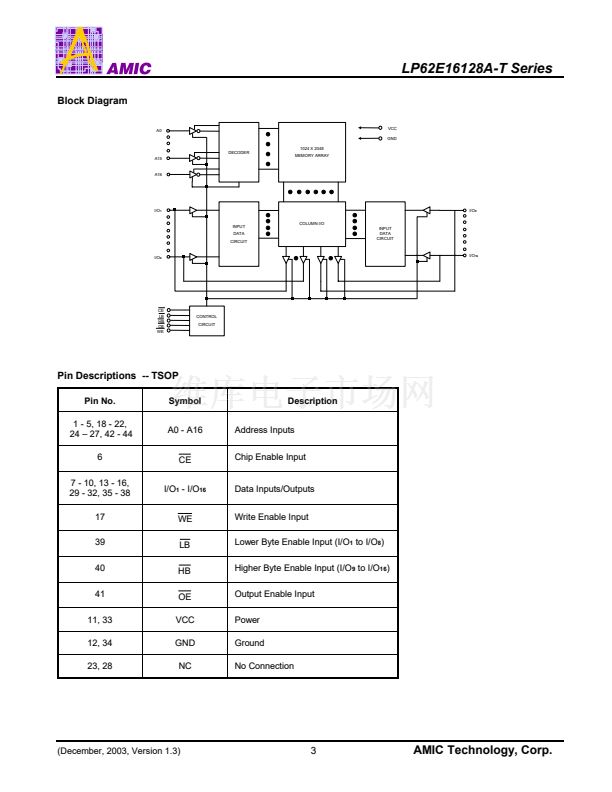
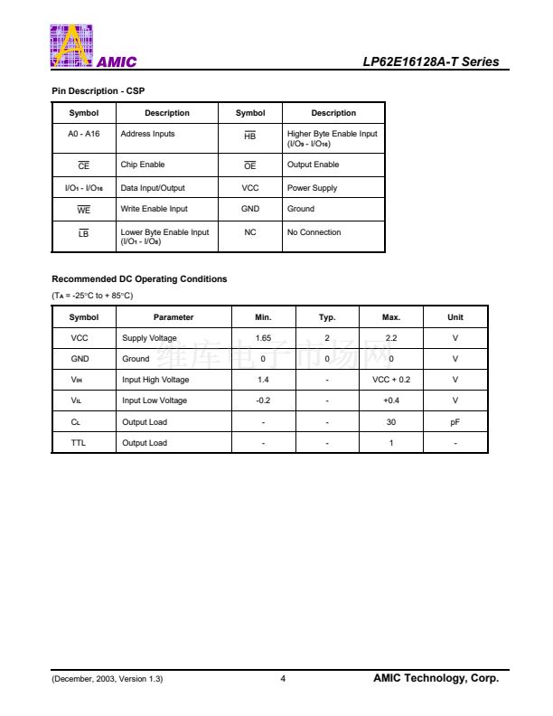
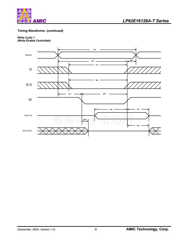
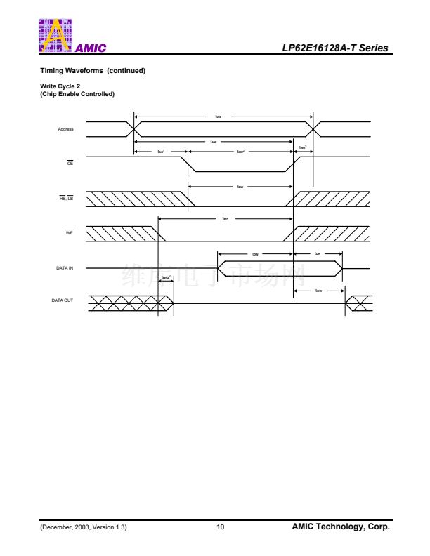
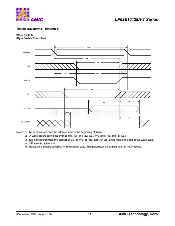
LP62E16128A-T Series
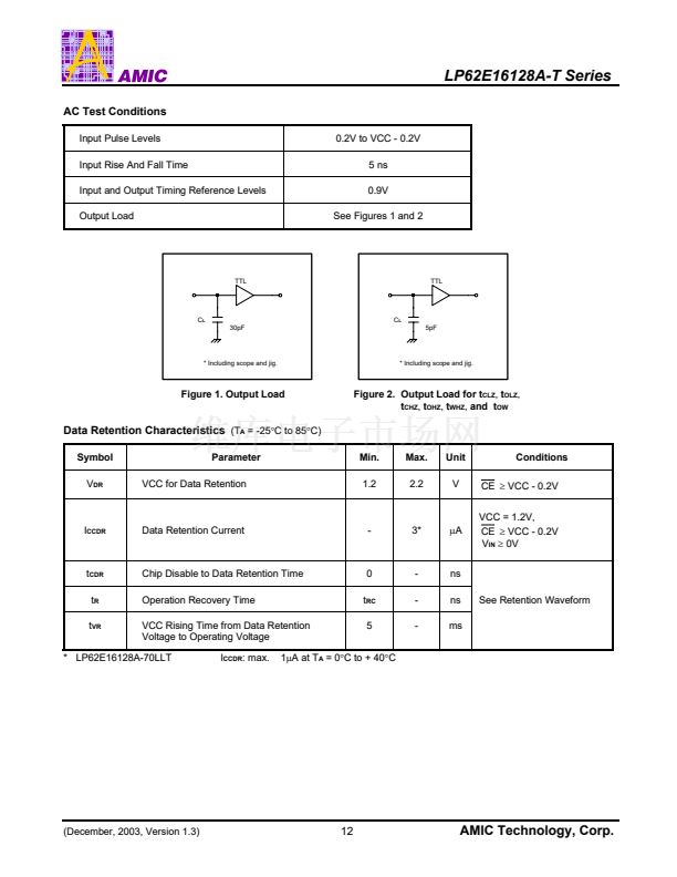
AC Test Conditions
Input Pulse Levels
Input Rise And Fall Time
Input and Output Timing Reference Levels
Output Load
0.2V to VCC - 0.2V
5 ns
0.9V
See Figures 1 and 2
TTL
TTL
C
L
30pF
C
L
5pF
* Including scope and jig.
* Including scope and jig.
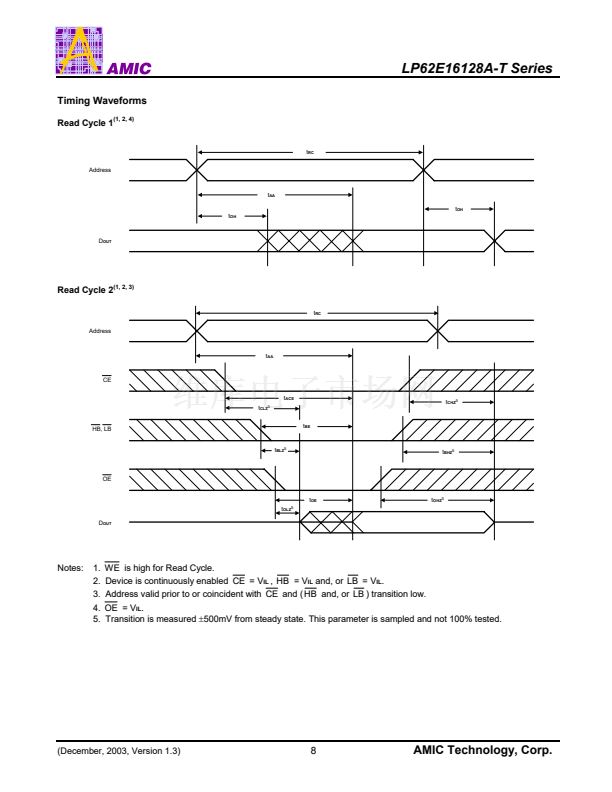
Figure 1. Output Load
Figure 2. Output Load for t
CLZ
,
t
OLZ
,
t
CHZ
,
t
OHZ
,
t
WHZ
,
and t
OW
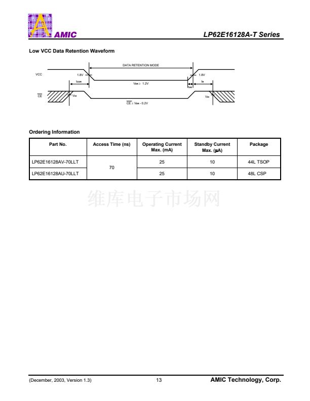
Data Retention Characteristics
(T
A
= -25
掳
C to 85
掳
C)
Symbol
V
DR
Parameter
VCC for Data Retention
Min.
1.2
Max.
2.2
Unit
V
Conditions
CE
鈮?/div>
VCC - 0.2V
VCC = 1.2V,
CE
鈮?/div>
VCC - 0.2V
V
IN
鈮?/div>
0V
I
CCDR
Data Retention Current
-
3*
碌
A
t
CDR
t
R
t
VR
Chip Disable to Data Retention Time
Operation Recovery Time
VCC Rising Time from Data Retention
Voltage to Operating Voltage
I
CCDR
: max.
0
t
RC
5
-
-
-
ns
ns
ms
See Retention Waveform
* LP62E16128A-70LLT
1
碌
A at T
A
= 0
掳
C to + 40
掳
C
(December, 2003, Version 1.3)
12
AMIC Technology, Corp.


 1
1
 2
2
 3
3
 4
4
 5
5
 6
6
 7
7
 8
8
 9
9
 10
10
 11
11
 12
12
 13
13
 14
14
 15
15
