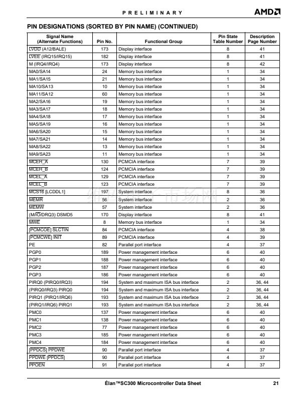
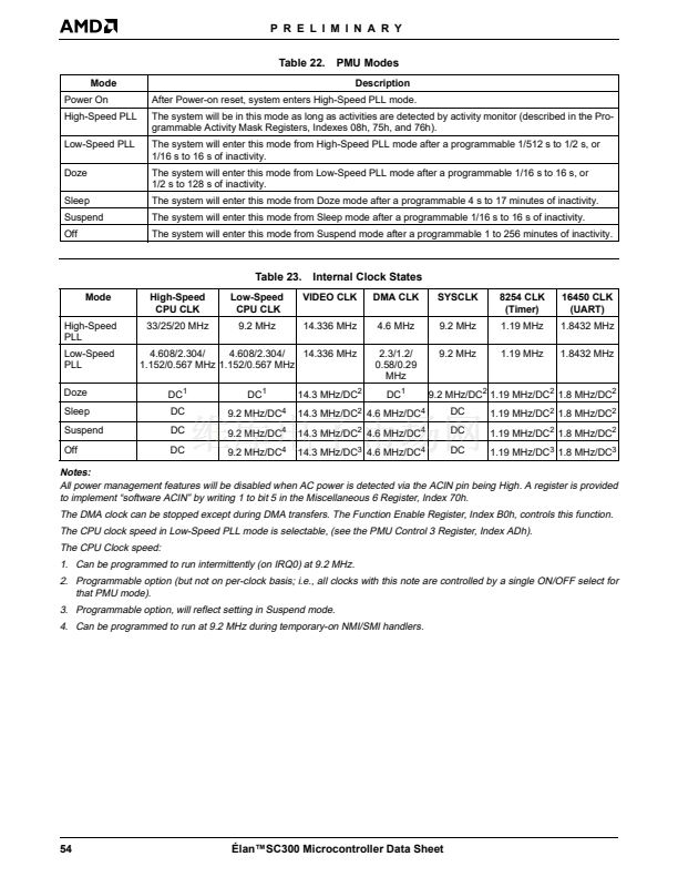
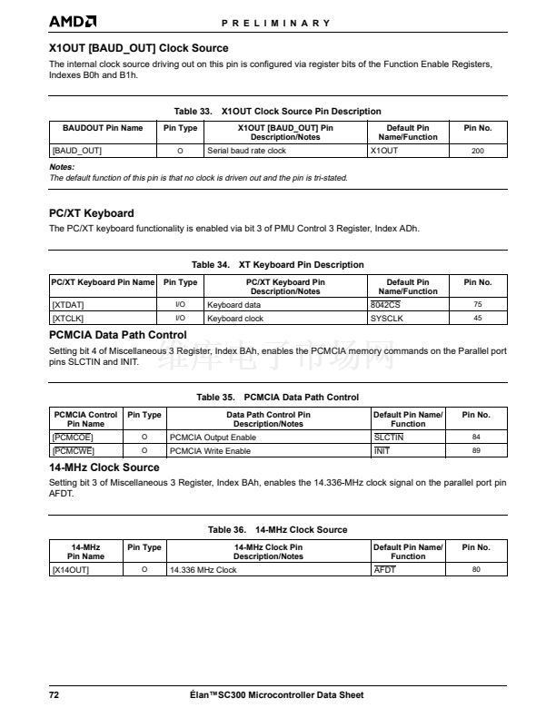
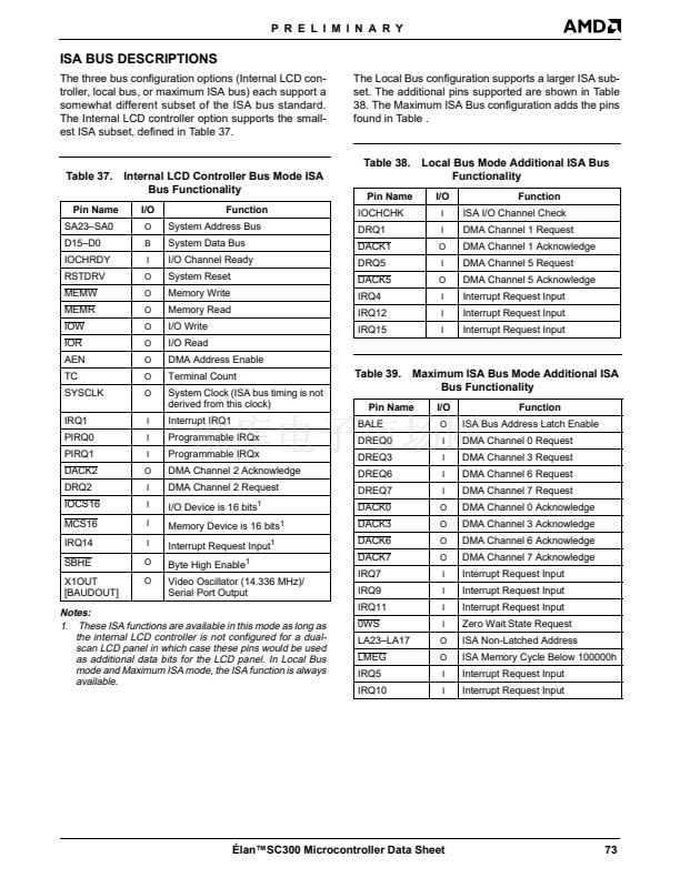
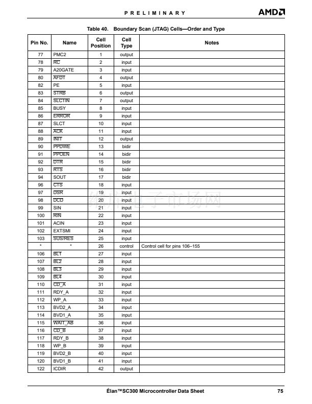
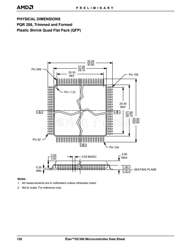
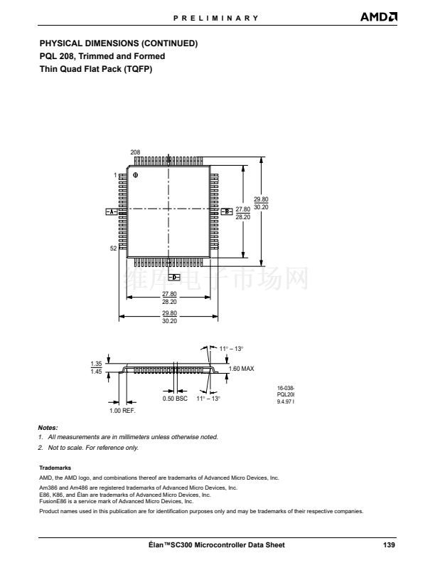
P R E L I M I N A R Y
For more information about the
ROMCS
pin, see the
Using 16-Bit
ROMCS
Designs in 脡lan
TM
SC300 and
脡lanSC310 Microcontrollers Application Note
, order
#21825.
This is a dual-function pin. When the JTAGEN signal is
asserted, it will function as the TDO, JTAG Test Data
Out pin. See 鈥淛TAG Boundary Scan Interface鈥?on page
44 for more information on the function of this pin dur-
ing Test mode.
ENDIRH
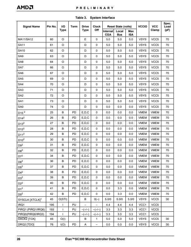
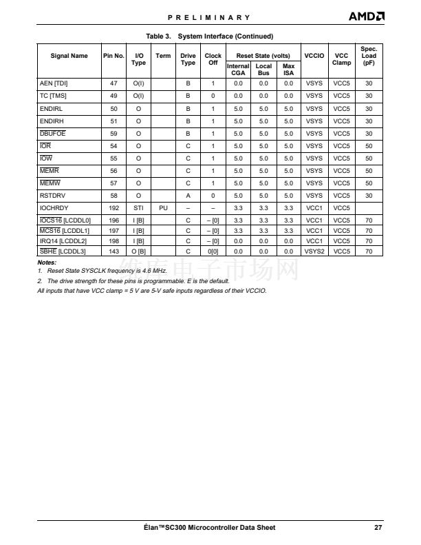
SYSTEM INTERFACE
AEN [TDI]
High Byte Data Buffer Direction Control
(Output; Active High)
This output controls the transceiver on the high byte of
the data bus, bits 15鈥?. When asserted, this signal is
used to enable the data from the 脡lanSC300 microcon-
troller data bus to the buffered data bus.
ENDIRL
DMA Address Enable (Output; Active High)
AEN is used to indicate that the current address active
on the SA23鈥揝A0 address bus is a memory address
and that the current cycle is a DMA cycle. All I/O de-
vices should use this signal in decoding their I/O ad-
dresses and should not respond when this signal is
asserted. When AEN is asserted, the DACKx signals
are used to select the appropriate I/O device for the
DMA transfer.
This is a dual-function pin. When the JTAGEN signal is
asserted, it functions as the TDI, JTAG Test Data Input
pin.
D15鈥揇0
Low Byte Data Buffer Direction Control
(Output; Active High)
This output controls the transceiver on the low byte of
the data bus, bits 7鈥?. When asserted, this signal is
used to enable the data from the 脡lanSC300 microcon-
troller data bus to the buffered data bus.
IOCHRDY
System Data Bus (Bidirectional; Active High)
The System Data Bus inputs data during memory and
I/O read cycles, and outputs data during memory and
I/O write cycles. During Local Bus and DRAM/SRAM
cycles, this bus represents the CPU data bus.
DACK2 [TCK]
I/O Channel Ready (Input; Active High)
This signal is used by ISA slave devices to add wait
states to the current transfer. When this signal is deas-
serted, wait states are added.
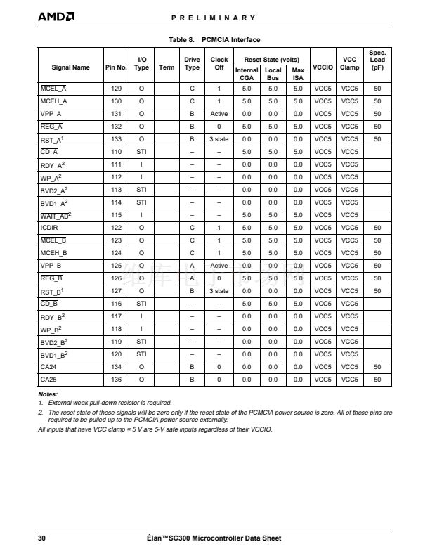
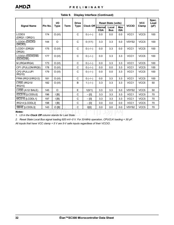
IOCS16 [LCDDL0]
(Input; Active Low)
This input is used to signal to the ISA control logic that
the targeted I/O device is a 16-bit device.
(IOCS16 is available unless the internal LCD Controller
Bus mode is selected and a dual-scan LCD panel inter-
face is selected via firmware.)
IOCS16
is generated by a 16-bit ISA I/O expansion
DMA Channel 2 Acknowledge (Output; Active Low)
This output indicates that the current transfer is a DMA
transfer to the I/O device connected to this DMA chan-
nel. In PC-compatible system designs, this signal can
be connected to the floppy disk controller DMA ac-
knowledge input.
This is a dual-function pin. When the JTAGEN signal is
asserted, it functions as the TCK (JTAG Test Clock)
pin. See 鈥淛TAG Boundary Scan Interface鈥?on page 44
for more information on the function of this pin during
Test mode.
DBUFOE
board when the board recognizes it is being ad-
dressed.
IOCS16
provides the same function for 16-bit
I/O expansion devices as the
MCS16
signal provides for
the 16-bit memory devices.
Note:
IOCS16
is internally OR鈥檇 with
MCS16
. Do not tie
IOCS16
Low.
For more information about the
IOCS16
pin, see the
Using 16-Bit
ROMCS
Designs in 脡lan
TM
SC300 and
脡lanSC310 Microcontrollers Application Note
, order
#21825.
IOR
Data Buffer Output Enable (Output; Active Low)
This output is used to control the output enable on the
system data bus buffer. When Low, the outputs of the
Data Bus Buffer are enabled.
DRQ2 [TDO]
DMA Channel 2 Request (Input; Active High
with Internal Pulldown)
This input is used to request a DMA transfer. It can be
connected to the floppy disk controller DMA request
output in PC-compatible system designs.
I/O Read Command (Output; Active Low)
The IOR signal indicates that the current cycle is a read
of the currently selected I/O device. When this signal is
asserted, the selected I/O device can drive data onto
the data bus.
脡lan鈩C300 Microcontroller Data Sheet
35


 1
1
 2
2
 3
3
 4
4
 5
5
 6
6
 7
7
 8
8
 9
9
 10
10
 11
11
 12
12
 13
13
 14
14
 15
15
 16
16
 17
17
 18
18
 19
19
 20
20
 21
21
 22
22
 23
23
 24
24
 25
25
 26
26
 27
27
 28
28
 29
29
 30
30
 31
31
 32
32
 33
33
 34
34
 35
35
 36
36
 37
37
 38
38
 39
39
 40
40
 41
41
 42
42
 43
43
 44
44
 45
45
 46
46
 47
47
 48
48
 49
49
 50
50
 51
51
 52
52
 53
53
 54
54
 55
55
 56
56
 57
57
 58
58
 59
59
 60
60
 61
61
 62
62
 63
63
 64
64
 65
65
 66
66
 67
67
 68
68
 69
69
 70
70
 71
71
 72
72
 73
73
 74
74
 75
75
 76
76
 77
77
 78
78
 79
79
 80
80
 81
81
 82
82
 83
83
 84
84
 85
85
 86
86
 87
87
 88
88
 89
89
 90
90
 91
91
 92
92
 93
93
 94
94
 95
95
 96
96
 97
97
 98
98
 99
99
 100
100
 101
101
 102
102
 103
103
 104
104
 105
105
 106
106
 107
107
 108
108
 109
109
 110
110
 111
111
 112
112
 113
113
 114
114
 115
115
 116
116
 117
117
 118
118
 119
119
 120
120
 121
121
 122
122
 123
123
 124
124
 125
125
 126
126
 127
127
 128
128
 129
129
 130
130
 131
131
 132
132
 133
133
 134
134
 135
135
 136
136
 137
137
 138
138
 139
139
