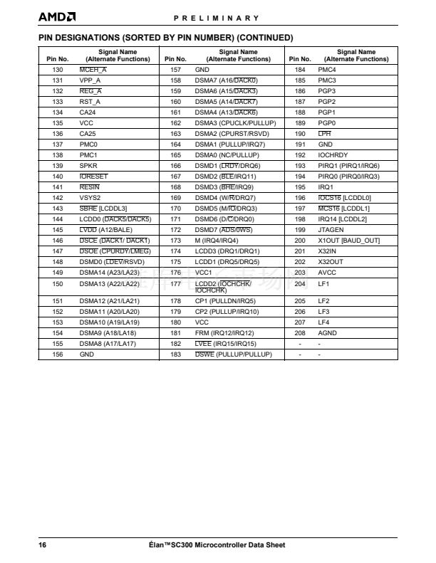
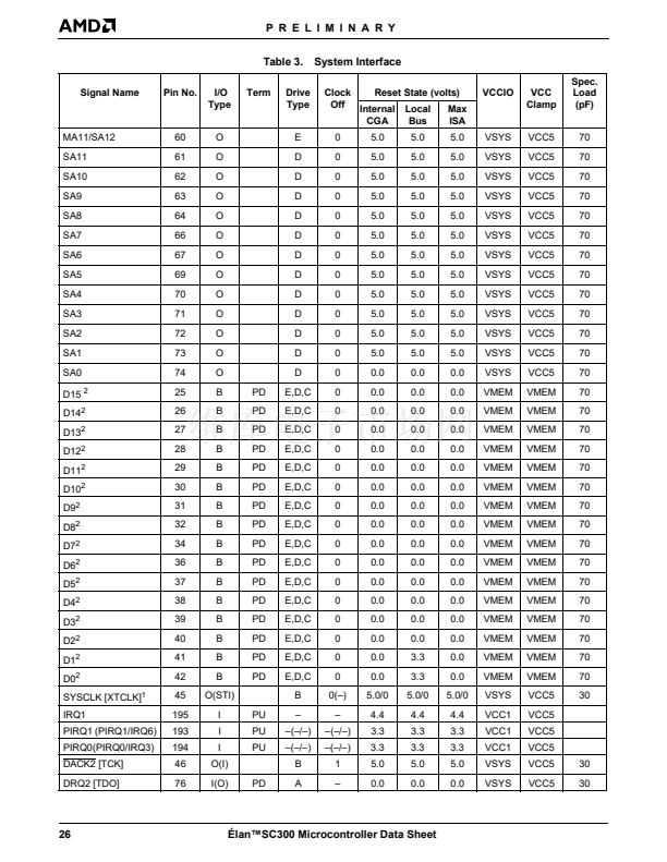
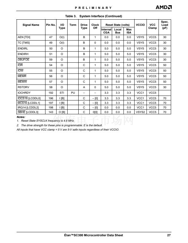
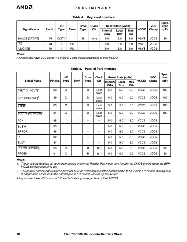
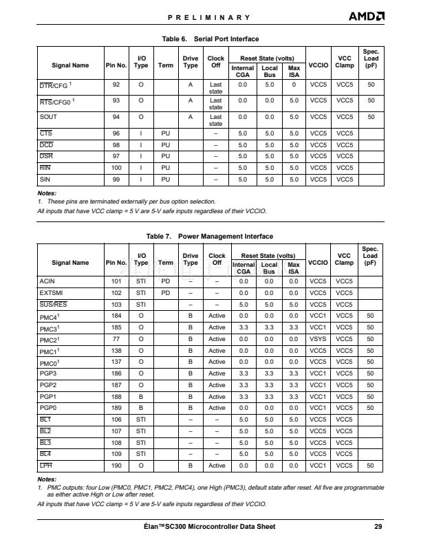
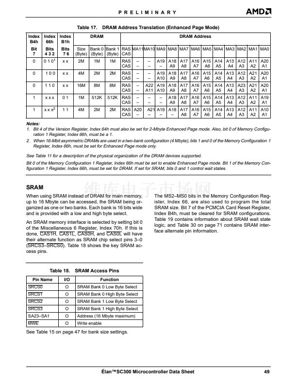
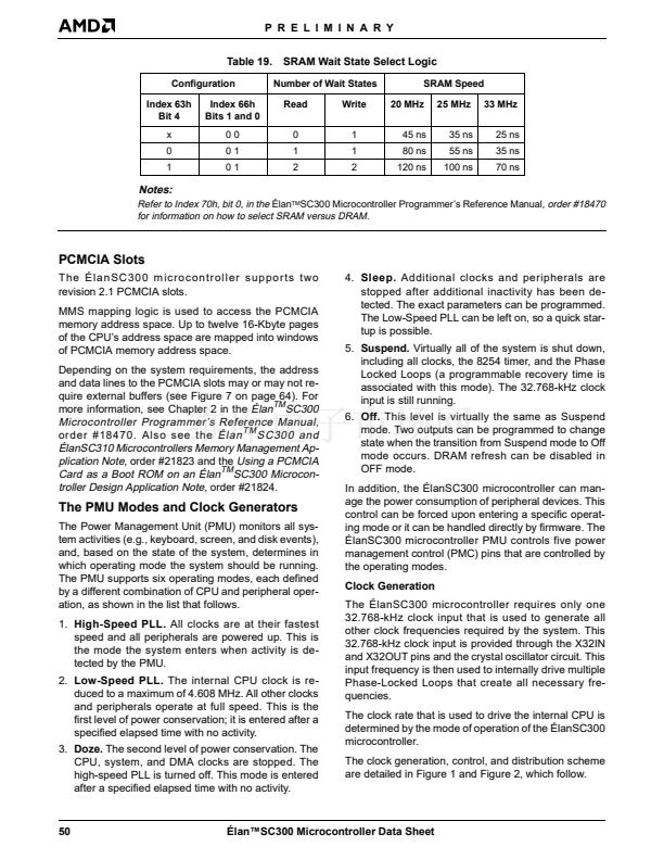
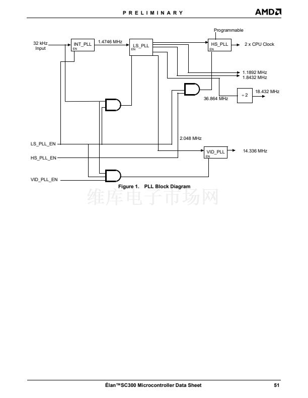
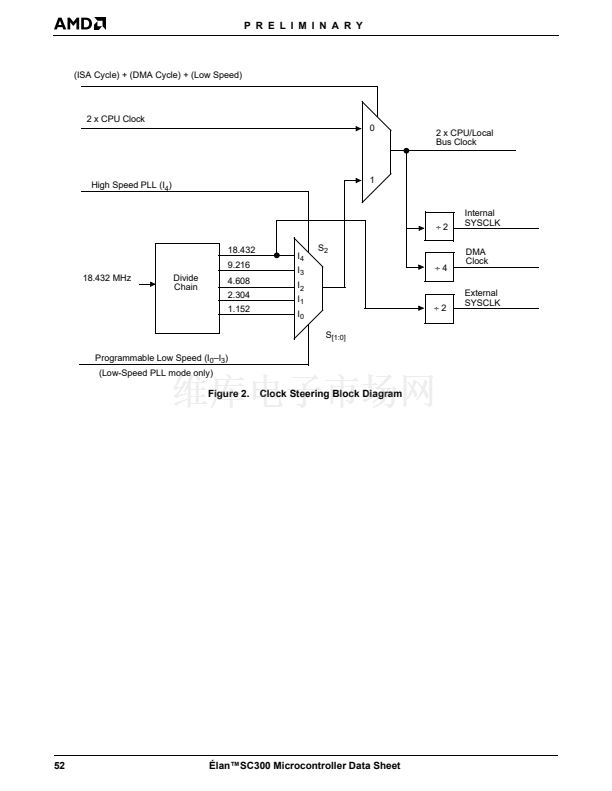
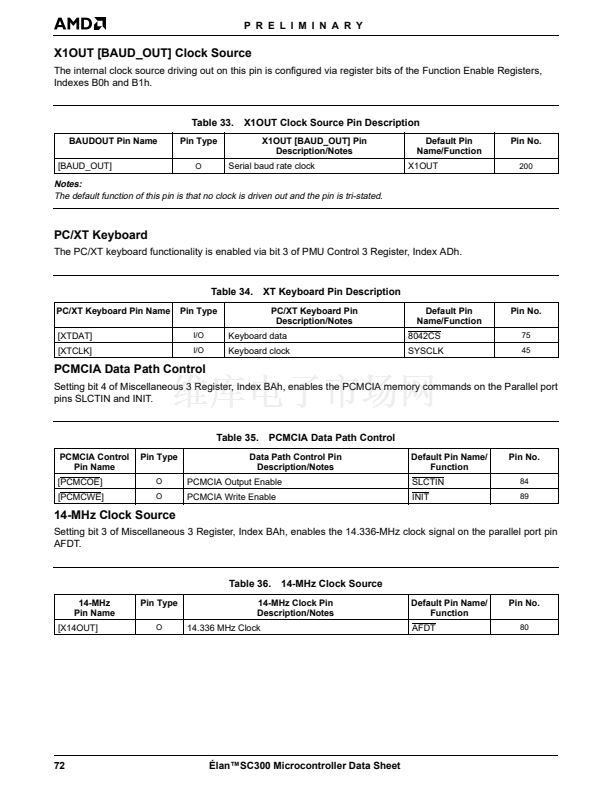
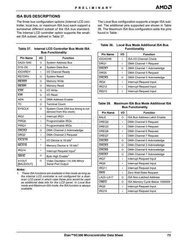
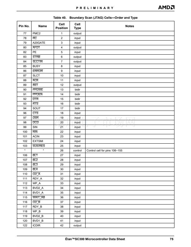
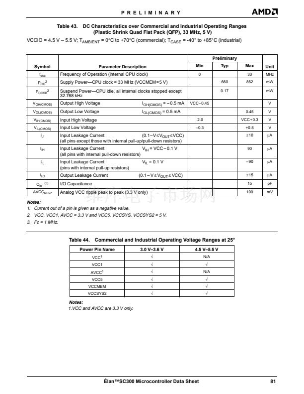
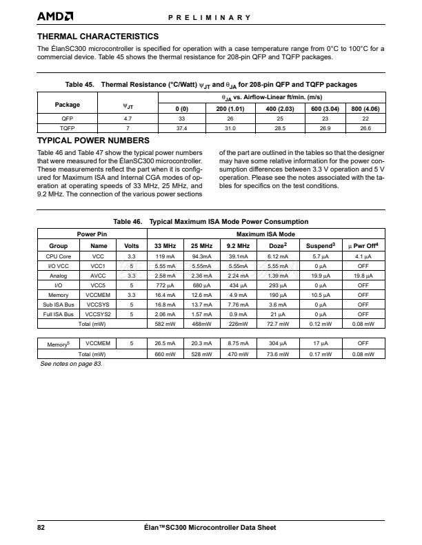
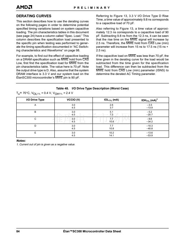
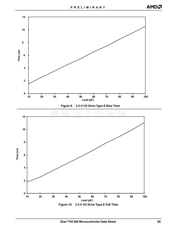
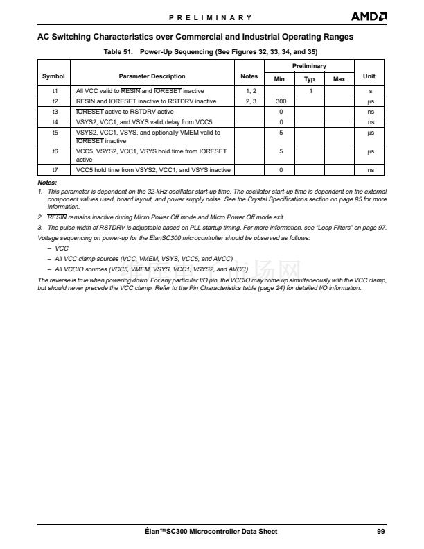
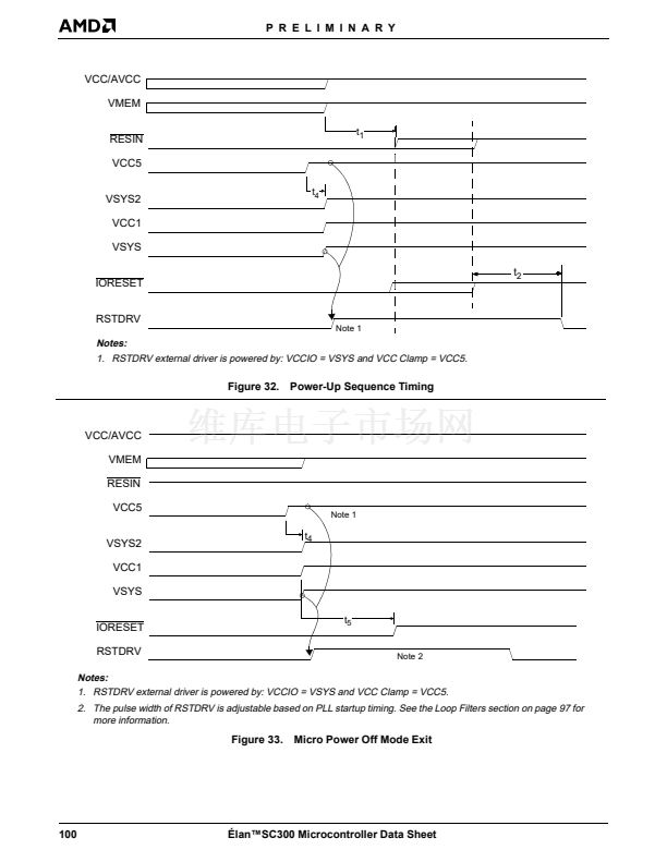
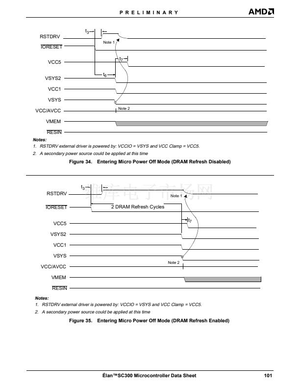
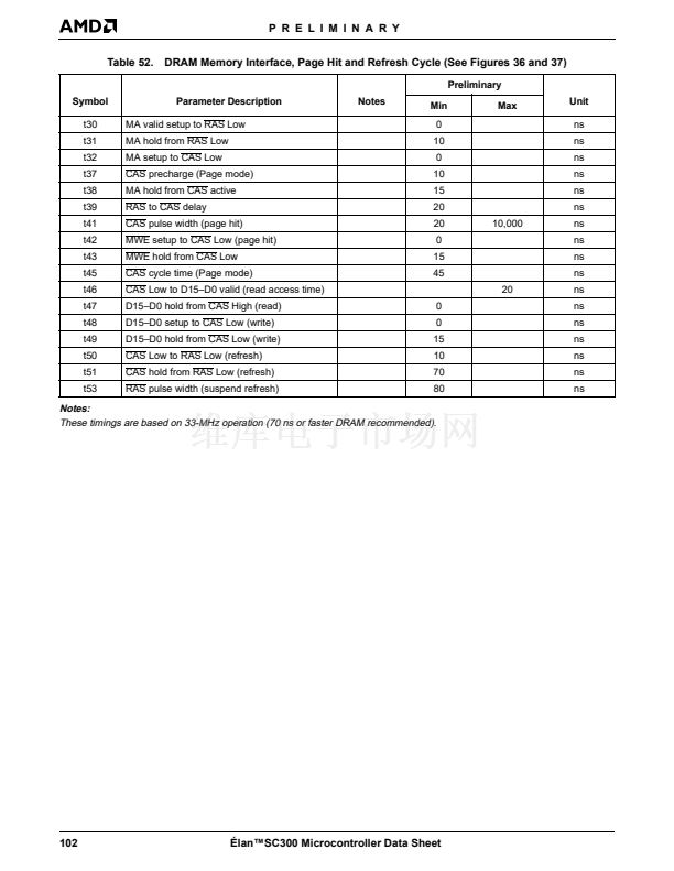
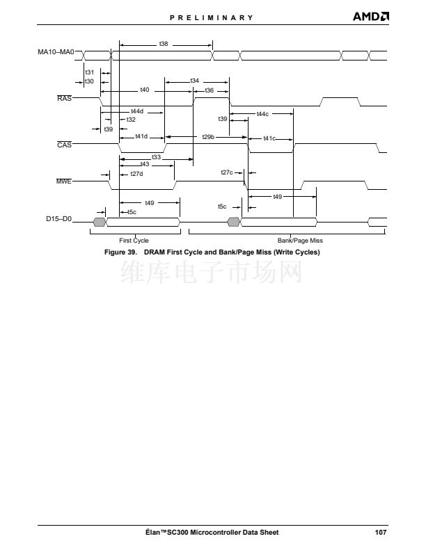
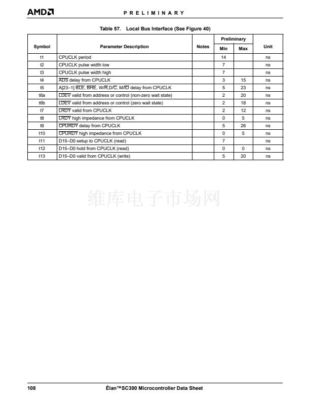
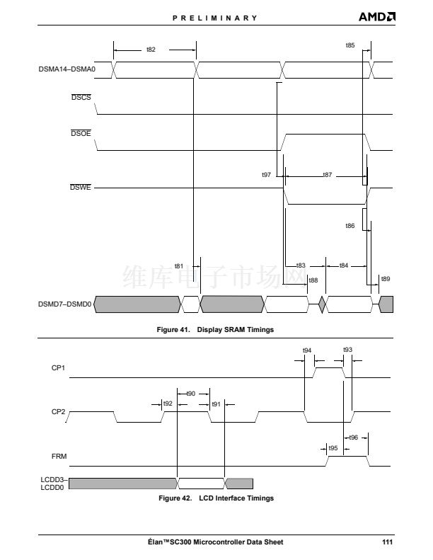
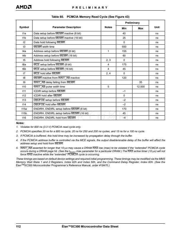
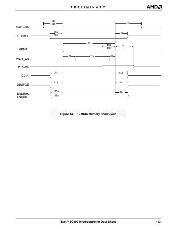
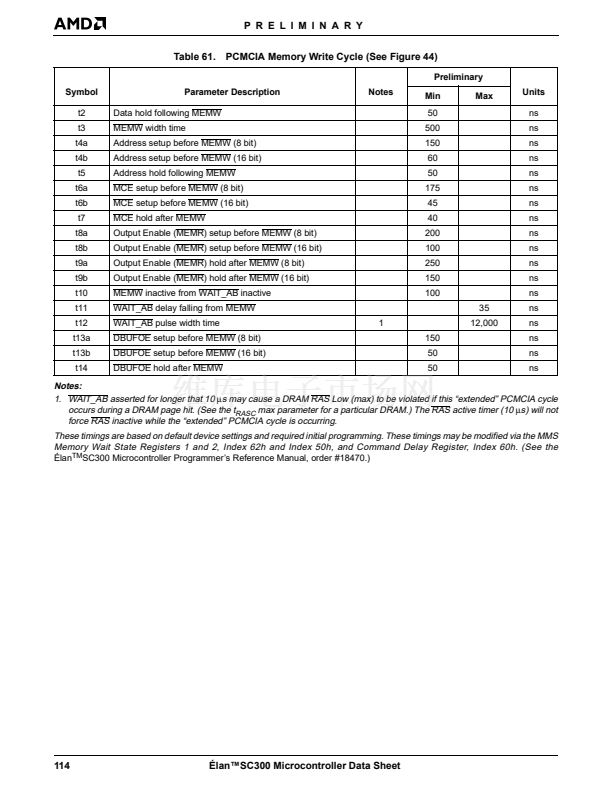
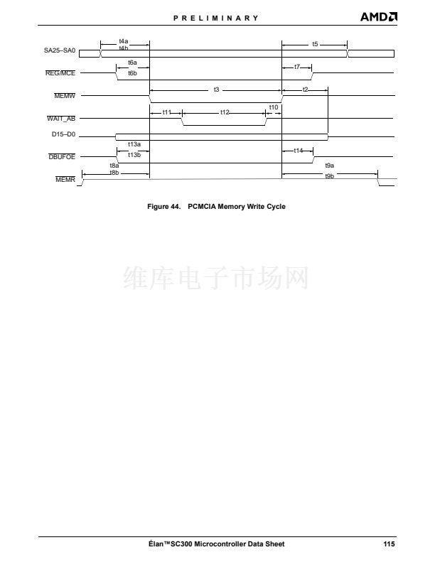
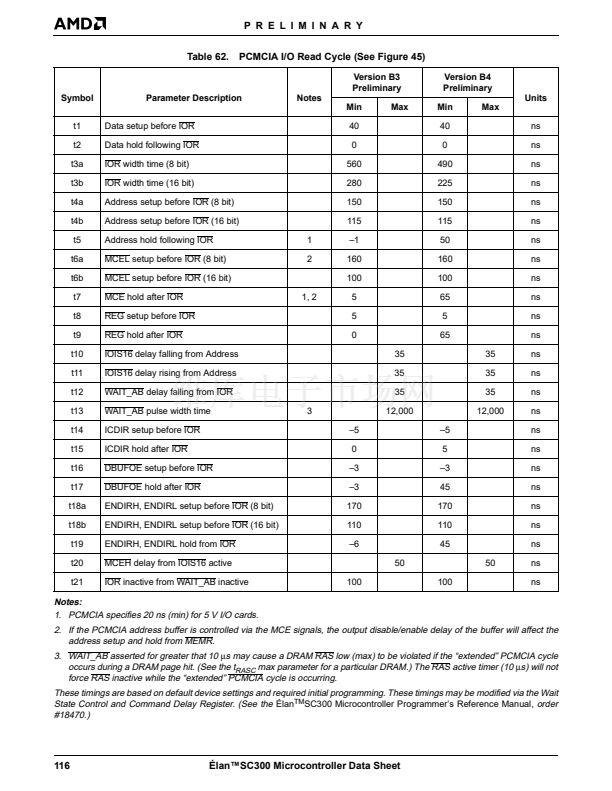
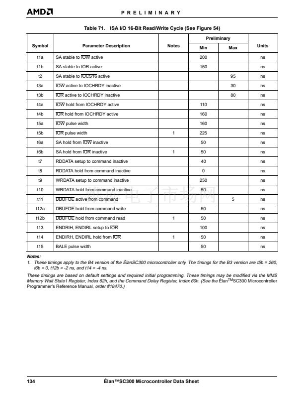
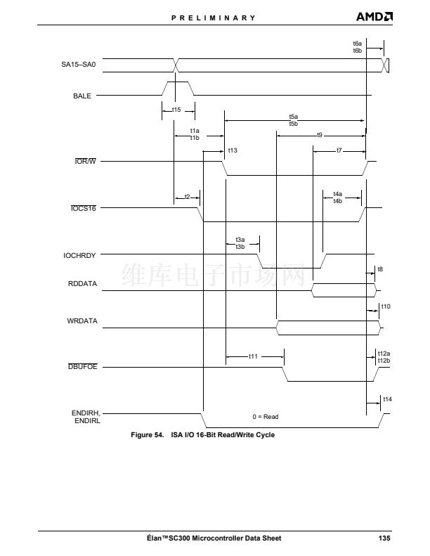
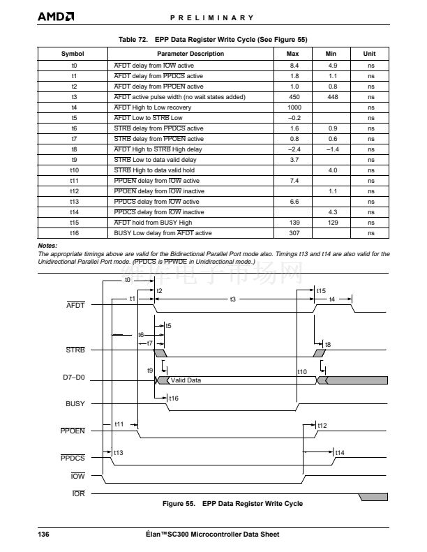
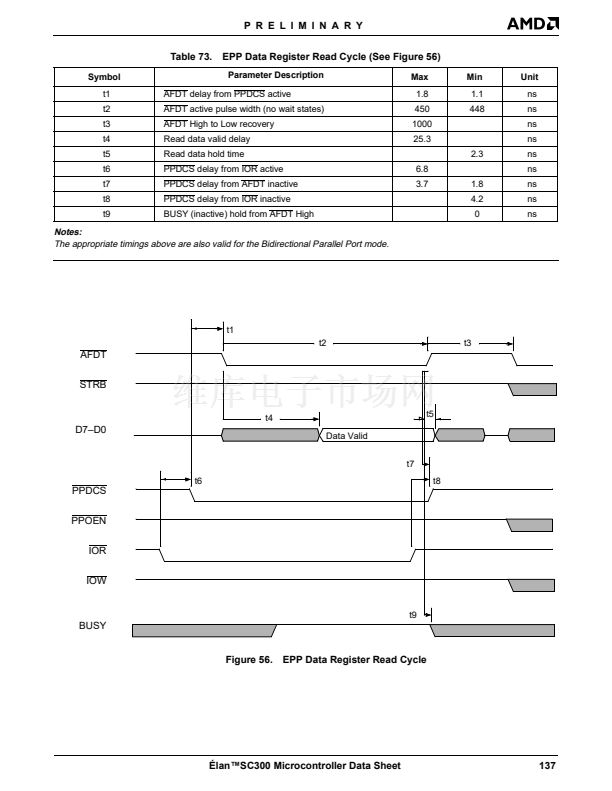
P R E L I M I N A R Y
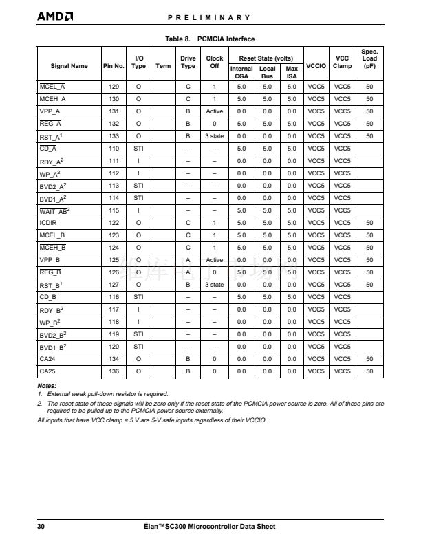
ICDIR
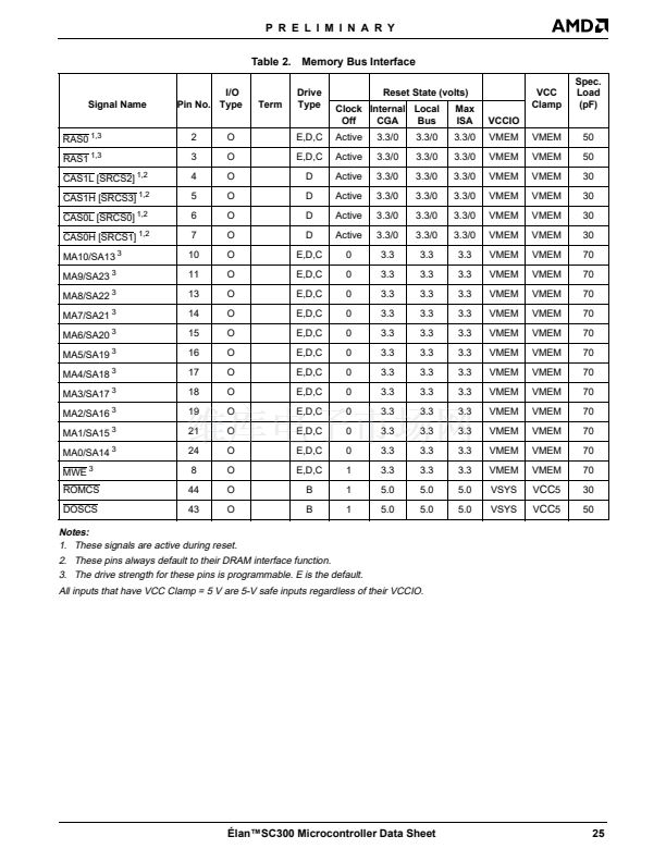
RST_A, RST_B
Card Data Direction (Output)
This signal controls the direction of the card data buff-
ers or translators, working in conjunction with the
MCEL_x
and
MCEH_x
card enable signals to control the
data buffers on the card interface. When this signal is
High, the data flow is from the 脡lanSC300 microcon-
troller to the card socket, indicating a data write cycle.
When this signal is Low, the data flow is from the card
socket into the 脡lanSC300 microcontroller, indicating a
read cycle. Note that PCMCIA bus buffering may or
may not be implemented in a system design.
MCEH_A, MCEH_B
Card Reset (Outputs; Active High)
These signals reset their respective cards. When ac-
tive, this signal clears the Card Configuration Option
register, thus placing a card in a memory-only mode.
VPP_A, VPP_B
Program and Peripheral Voltage Control
(Output; Active High)
These signals can be used to enable the programming
voltages to their respective card interfaces.
WAIT_AB
Extend Bus Cycle (Input; Active Low)
This signal delays the completion of the memory ac-
cess or I/O access that is currently in progress. When
this signal is asserted (Low), wait states will be inserted
into the cycle in progress. A two-card solution needs
each slot鈥檚 WAIT_AB signal 鈥淎NDed鈥?before being
input to the 脡lanSC300 microcontroller.
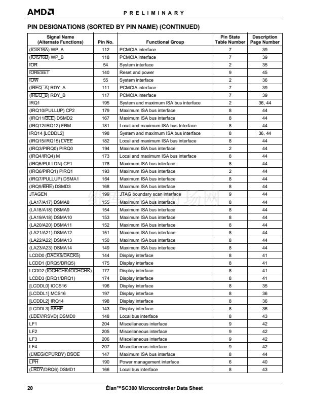
WP_A (IOIS16A), WP_B (IOIS16B)
Card Enables, High Byte (Output; Active Low)
These signals enable odd address bytes for their re-
spective card interfaces.
MCEL_A, MCEL_B
Card Enables, Low Byte (Output; Active Low)
These signals enable even address bytes for their re-
spective card interfaces.
PCMCOE
Write Protect (Inputs; Active High)
When a memory interface is selected, this signal indi-
cates the status of the targeted device鈥檚 Write Protect
Switch. When the targeted device is configured for an
I/O interface, the WP_A signal is used to indicate that
the currently accessed port is a 16-bit port (IOIS16x ac-
tive Low).
Both WP_A and WP_B signals indicate that the tar-
geted device is a 16-bit device during I/O access to the
targeted device. When the targeted device is config-
ured as an I/O access, the two signals are OR鈥檇 to-
gether to generate the
IOIS16x
signal. When the
targeted device is configured as an I/O access, there is
basically no difference between the WP_A and WP_B
signals.
Card Memory Output Enable (Output, Active Low)
The Parallel Port SLCTIN signal can be programmed to
become PCMCOE. PCMCOE indicates that a memory
read cycle from the card interface is being performed.
PCMCWE
Card Memory Write Enable (Output, Active Low)
The Parallel Port INIT signal can be programmed to be-
come PCMCWE. PCMCWE indicates that a memory
write cycle to the card interface is being performed.
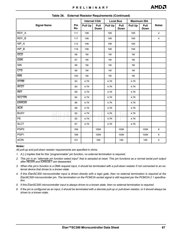
RDY_A (IREQ_A), RDY_B (IREQ_B)
Card Ready (Inputs; Active High)
This signal indicates that the respective card is ready
to accept a new data transfer command if a memory in-
terface is selected. If the card interface is configured as
an I/O interface, the Socket A I/O card鈥檚 IREQ_A signal
uses RDY_A as a general purpose input pin that may
be used as the card interrupt request input into the
脡lanSC300 microcontroller (active High). For more in-
formation about socket A card鈥檚 IREQ_A signal, see
Chapter 5 in the
脡lan
TM
SC300 Microcontroller Pro-
grammer鈥檚 Reference Manual
, order #18470.
REG_A, REG_B
Attribute Memory Select (Output; Active Low)
This signal selects either the Attribute Memory or the
Common Memory. This signal will be inactive (High) for
accesses to Common Memory, and asserted (Low) for
accesses to Attribute Memory. This signal is also as-
serted (Low) for all I/O accesses.
脡lan鈩C300 Microcontroller Data Sheet
39


 1
1
 2
2
 3
3
 4
4
 5
5
 6
6
 7
7
 8
8
 9
9
 10
10
 11
11
 12
12
 13
13
 14
14
 15
15
 16
16
 17
17
 18
18
 19
19
 20
20
 21
21
 22
22
 23
23
 24
24
 25
25
 26
26
 27
27
 28
28
 29
29
 30
30
 31
31
 32
32
 33
33
 34
34
 35
35
 36
36
 37
37
 38
38
 39
39
 40
40
 41
41
 42
42
 43
43
 44
44
 45
45
 46
46
 47
47
 48
48
 49
49
 50
50
 51
51
 52
52
 53
53
 54
54
 55
55
 56
56
 57
57
 58
58
 59
59
 60
60
 61
61
 62
62
 63
63
 64
64
 65
65
 66
66
 67
67
 68
68
 69
69
 70
70
 71
71
 72
72
 73
73
 74
74
 75
75
 76
76
 77
77
 78
78
 79
79
 80
80
 81
81
 82
82
 83
83
 84
84
 85
85
 86
86
 87
87
 88
88
 89
89
 90
90
 91
91
 92
92
 93
93
 94
94
 95
95
 96
96
 97
97
 98
98
 99
99
 100
100
 101
101
 102
102
 103
103
 104
104
 105
105
 106
106
 107
107
 108
108
 109
109
 110
110
 111
111
 112
112
 113
113
 114
114
 115
115
 116
116
 117
117
 118
118
 119
119
 120
120
 121
121
 122
122
 123
123
 124
124
 125
125
 126
126
 127
127
 128
128
 129
129
 130
130
 131
131
 132
132
 133
133
 134
134
 135
135
 136
136
 137
137
 138
138
 139
139
