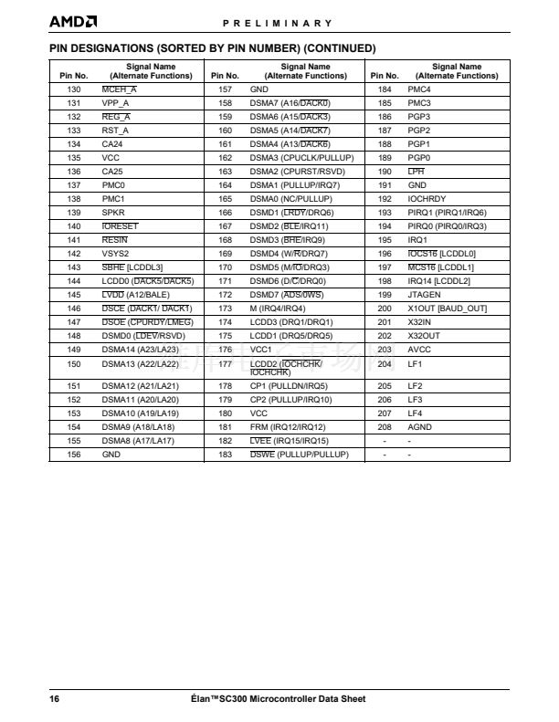
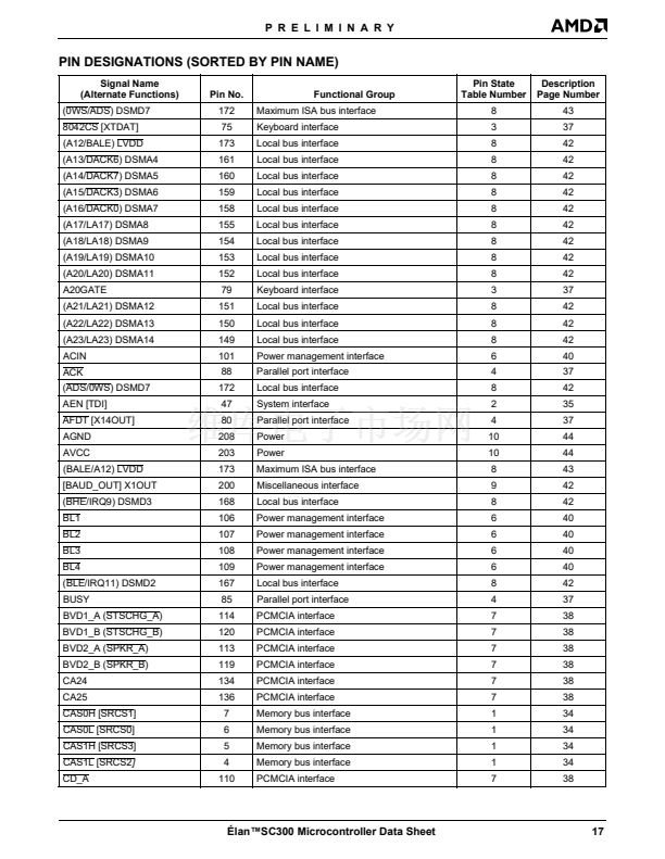
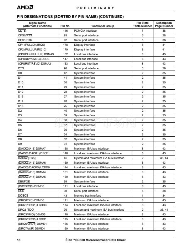
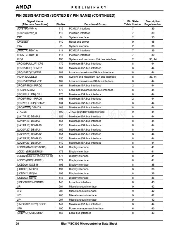
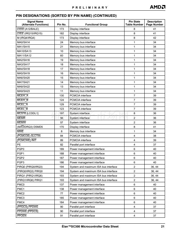
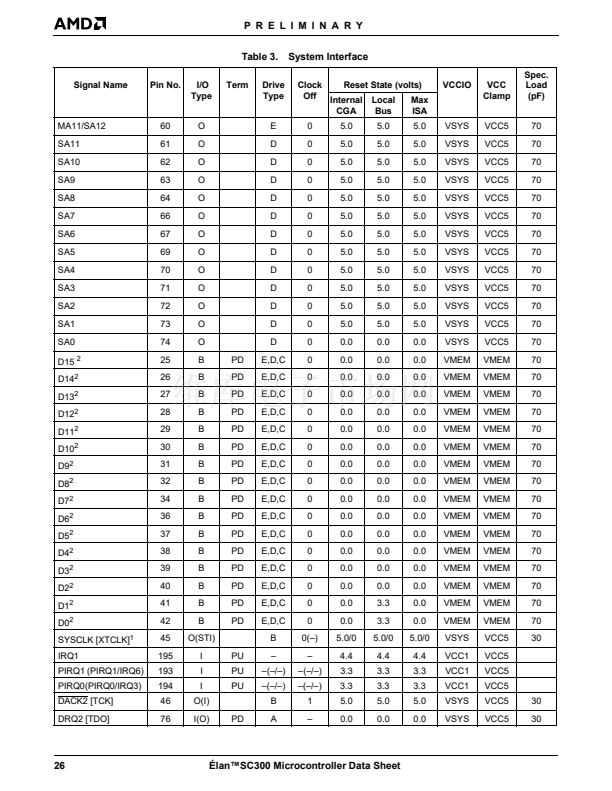
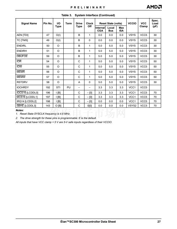
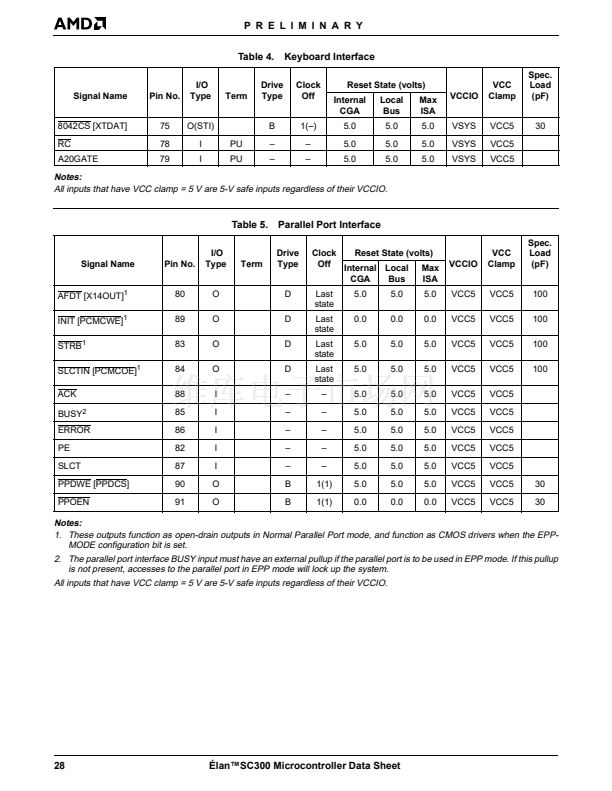
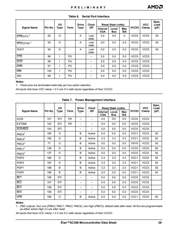
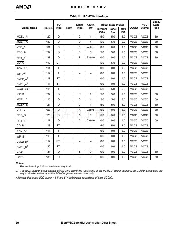
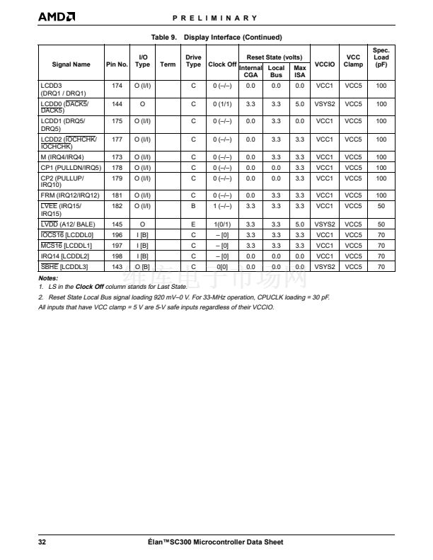
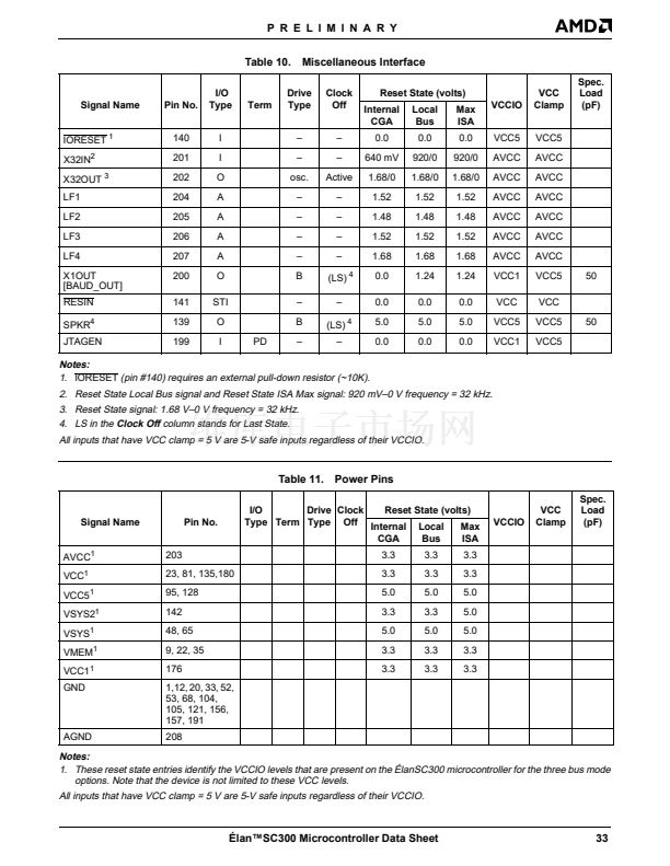
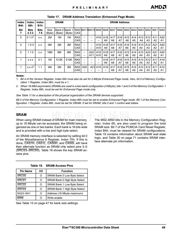
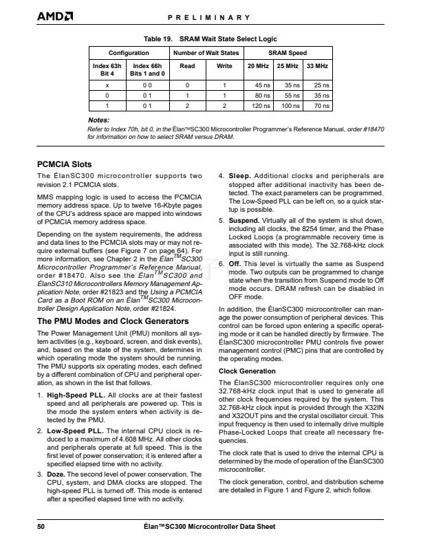
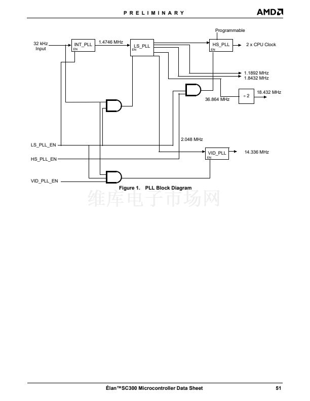
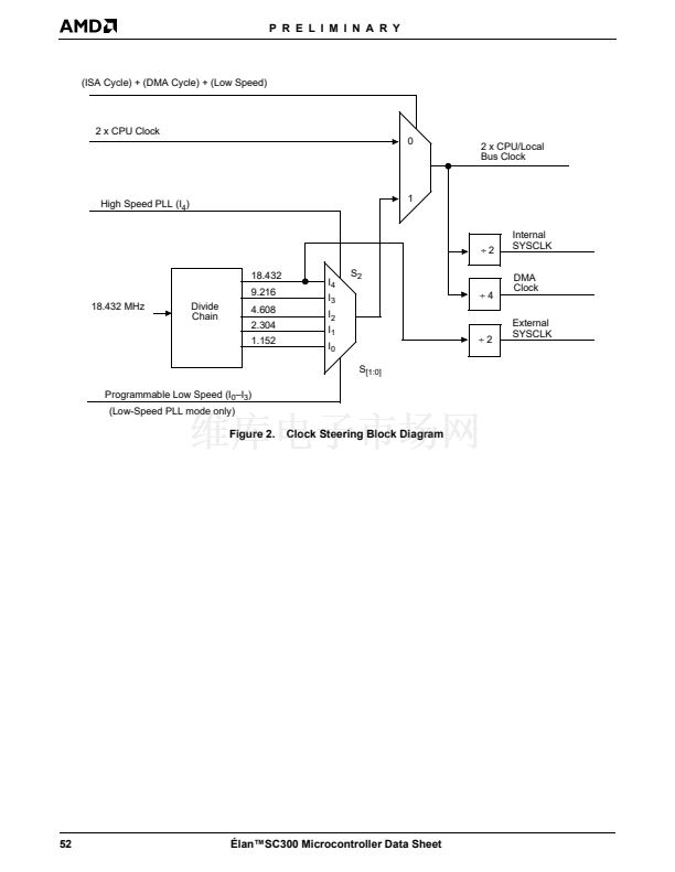
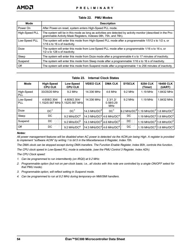
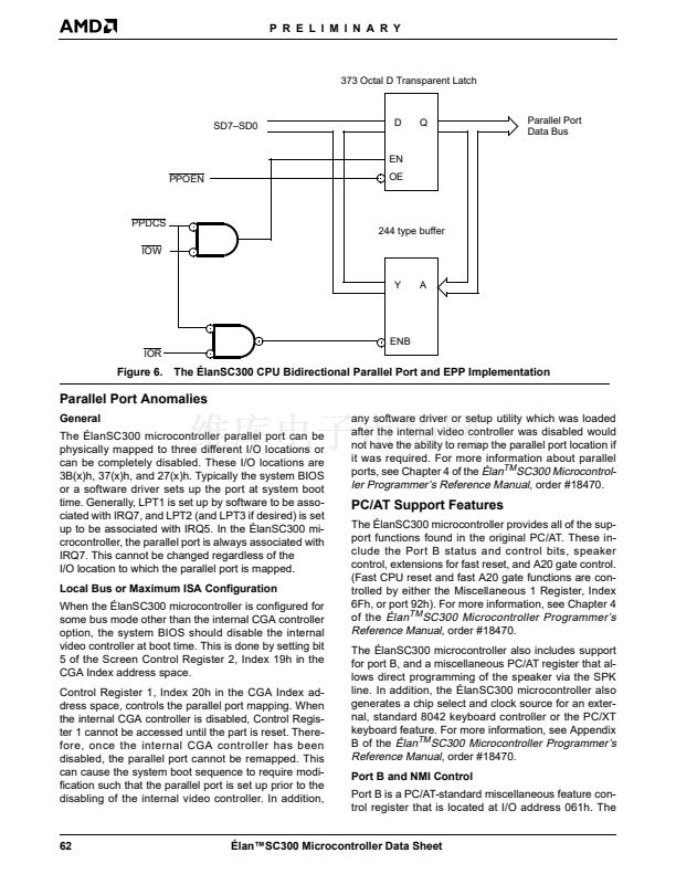
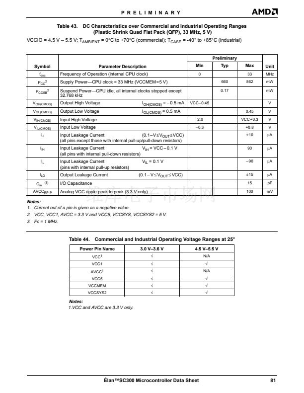
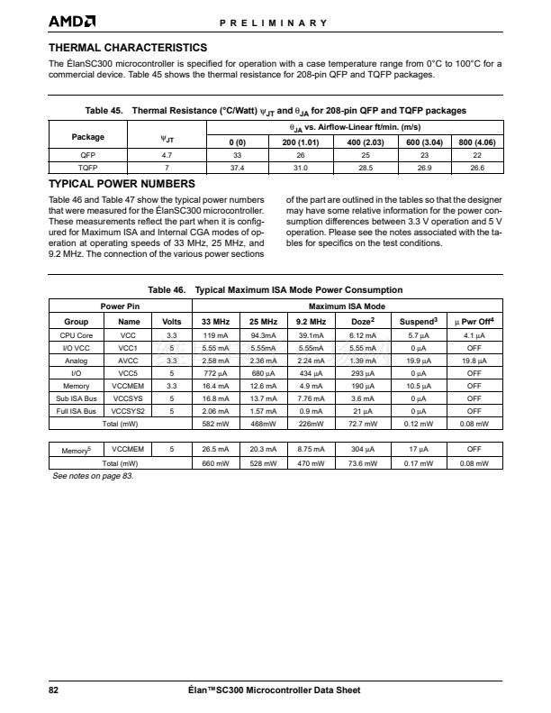
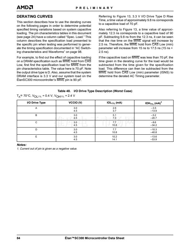
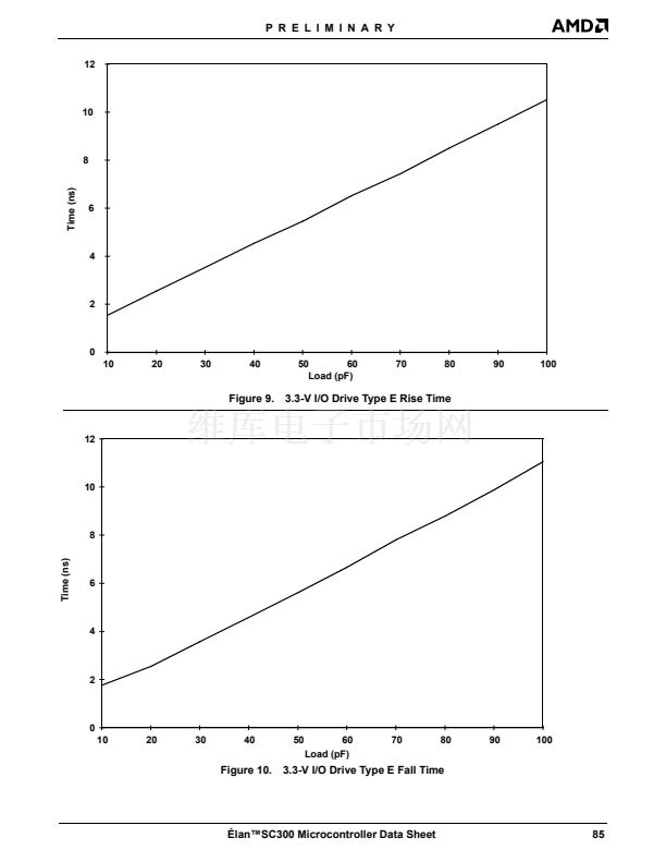
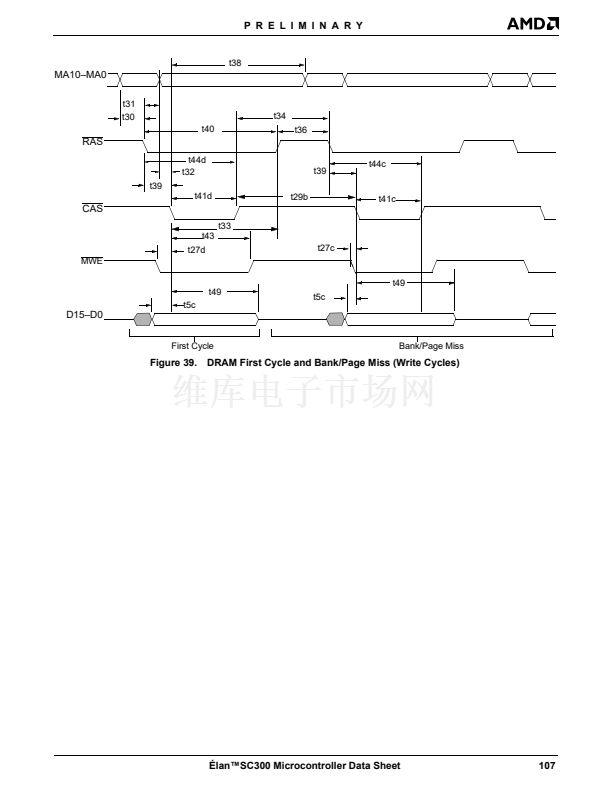
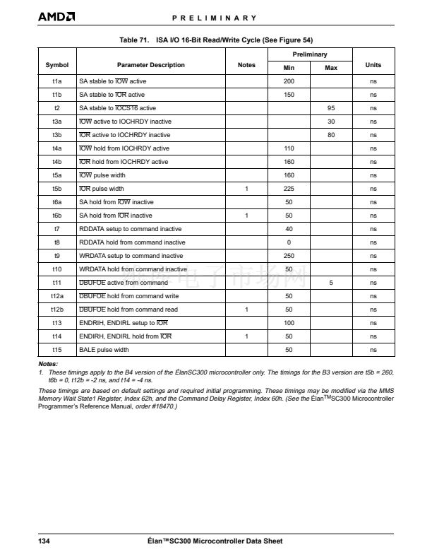
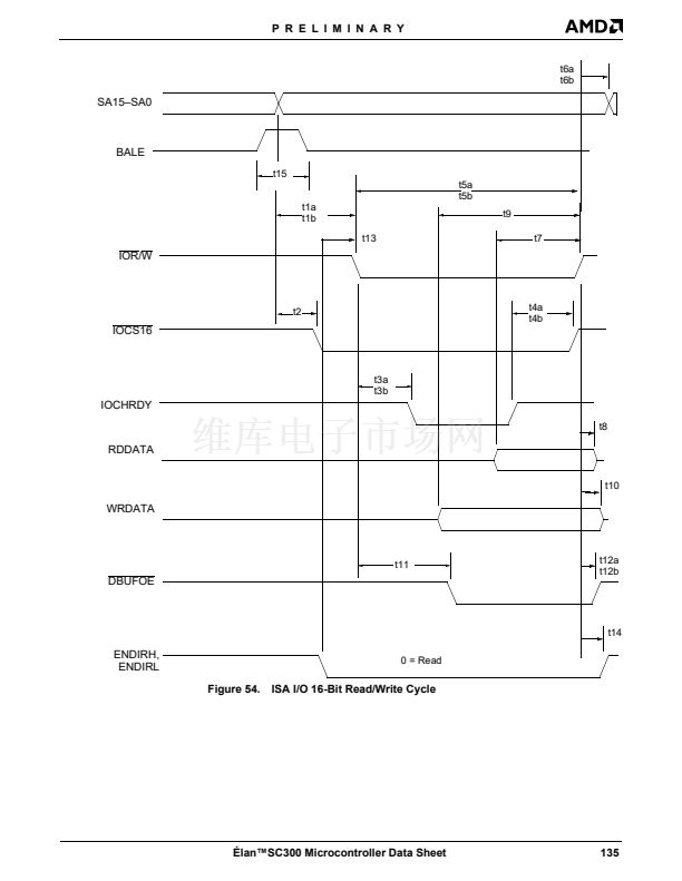
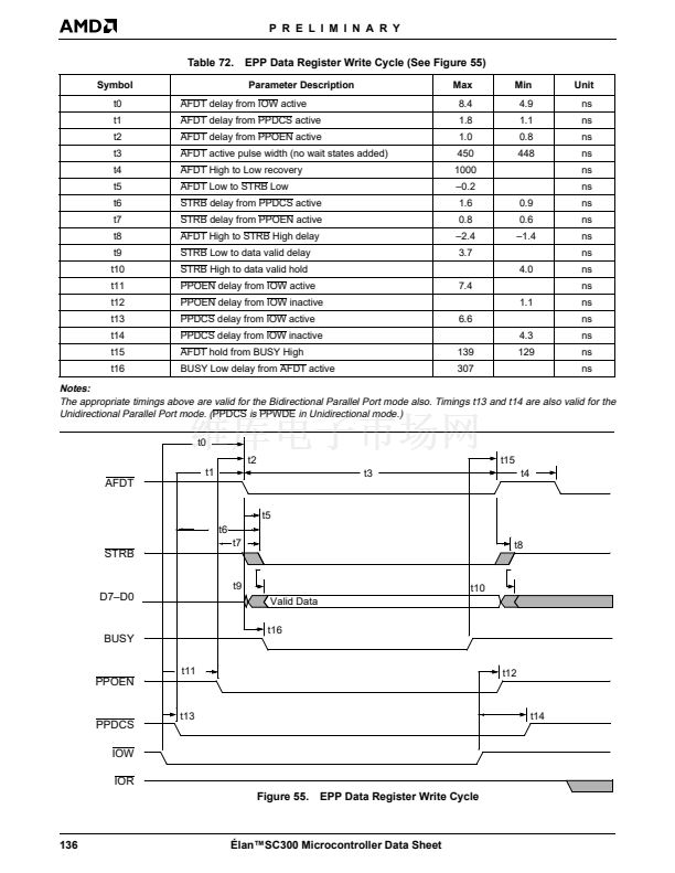
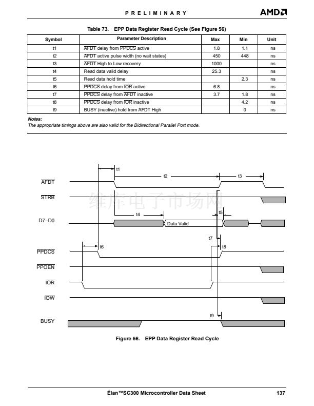
P R E L I M I N A R Y
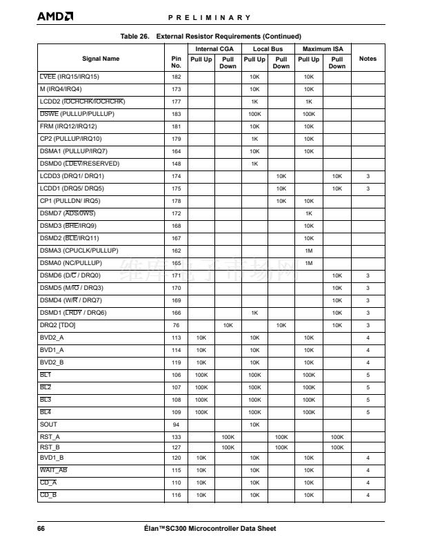
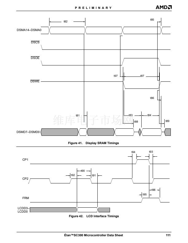
CP1
LCDD1
LCD Panel Line Clock (Output)
This is the Line Clock when in internal LCD mode and
an LCD configuration is selected. It is activated at the
start of every pixel line refresh cycle. CP1 should be
connected to the equivalent line on the LCD panel.
CP2
LCD Data Bit (Output)
When in internal LCD mode and an LCD configuration
is selected, this signal is data bit 1. LCDD1 should be
connected to the corresponding pin on the LCD panel.
LCDD2
LCD Data Bit (Output)
When in internal LCD mode and an LCD configuration
is selected, this signal is data bit 2. LCDD2 should be
connected to the corresponding pin on the LCD panel.
LCDD3
LCD Panel Shift Clock (Output)
This is the nibble/byte strobe when in internal LCD
mode and an LCD configuration is selected. CP2 is
also known as the shift clock or data shift. It is used by
the LCD to latch data. CP2 should be connected to the
equivalent line on the LCD panel.
DSCE
LCD Data Bit (Output)
When in internal LCD mode and an LCD configuration
is selected, this signal is data bit 3. LCDD3 is the MSB
and should be connected to the corresponding MSB
pin on the LCD panel.
[LCDDL3鈥揕CDDL0]
Display SRAM Chip Enable (Output; Active Low)
This signal generates the external video SRAM Chip
Enable.
DSMA14鈥揇SMA0
Display SRAM Address Bus (Output)
These signals generate the address to the SRAM. Up
to 32 Kbyte can be supported for the display interface.
DSMD7鈥揇SMD0
LCD Panel Data Bits for Dual-Scan Panels
(Outputs)
When the 脡lanSC300 microcontroller is programmed
to support LCD Dual-Scan Panel mode (separate data
bits for the top and bottom half of the panel), these bits
(LCDDL3鈥揕CDDL0) are for the bottom half of the
screen. LCDD3鈥揕CDD0 are the data bits for the top
half of the screen. LCD Dual-Scan Panel mode is se-
lected via firmware. LCDDL0 is the LSB for the lower
panel and LCDDL3 is the MSB for the lower panel.
These pins are shared with IOCS16, MCS16, IRQ14,
and SBHE (described in 鈥淪ystem Interface鈥? beginning
on page 35.) LCDDL3鈥揕CDDL0 should be connected
to their corresponding pins on the dual-screen LCD
lower panel.
LVDD
Display SRAM Data Bus (Bidirectional)
These signals provide the data bus used for the video
SRAM.
DSOE
Display SRAM Output Enable (Output; Active Low)
This signal controls the video SRAM Output Enable
pin.
DSWE
Display SRAM Write Enable (Output; Active Low)
When asserted, this signal indicates a Write to the
video SRAM.
FRM
LCD Panel VDD Voltage Control
(Output; Active Low)
This signal is used to control the assertion of the LCD鈥檚
VDD driver. LVDD is provided to be part of the solution
in sequencing the panel鈥檚 VDD, DATA, and VEE sig-
nals in the proper order.
LVEE
LCD Panel Line Frame Start (Output)
This signal is asserted at the start of every frame (panel
scan) when in LCD mode and an LCD configuration is
selected. FRM is also known as FLM or frame. It should
be connected to the equivalent line on the LCD panel.
LCDD0
LCD Panel VEE Voltage Control
(Output; Active Low)
This signal is used to control the assertion of the LCD鈥檚
VEE driver. LVEE is provided to be part of the solution
in sequencing the panel鈥檚 VDD, DATA, and VEE sig-
nals in the proper order.
LCD Data Bit (Output)
When in internal LCD mode and an LCD configuration
is selected, this signal is data bit 0. LCDD0 is the LSB
and should be connected to the corresponding LSB pin
on the LCD panel.
脡lan鈩C300 Microcontroller Data Sheet
41


 1
1
 2
2
 3
3
 4
4
 5
5
 6
6
 7
7
 8
8
 9
9
 10
10
 11
11
 12
12
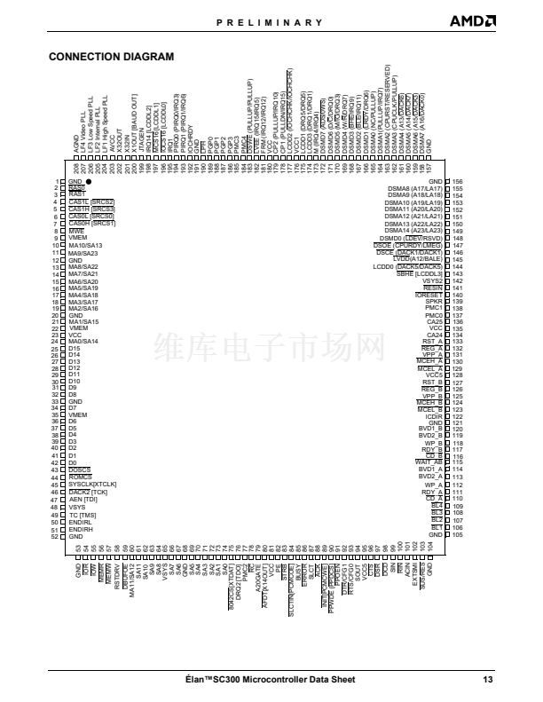 13
13
 14
14
 15
15
 16
16
 17
17
 18
18
 19
19
 20
20
 21
21
 22
22
 23
23
 24
24
 25
25
 26
26
 27
27
 28
28
 29
29
 30
30
 31
31
 32
32
 33
33
 34
34
 35
35
 36
36
 37
37
 38
38
 39
39
 40
40
 41
41
 42
42
 43
43
 44
44
 45
45
 46
46
 47
47
 48
48
 49
49
 50
50
 51
51
 52
52
 53
53
 54
54
 55
55
 56
56
 57
57
 58
58
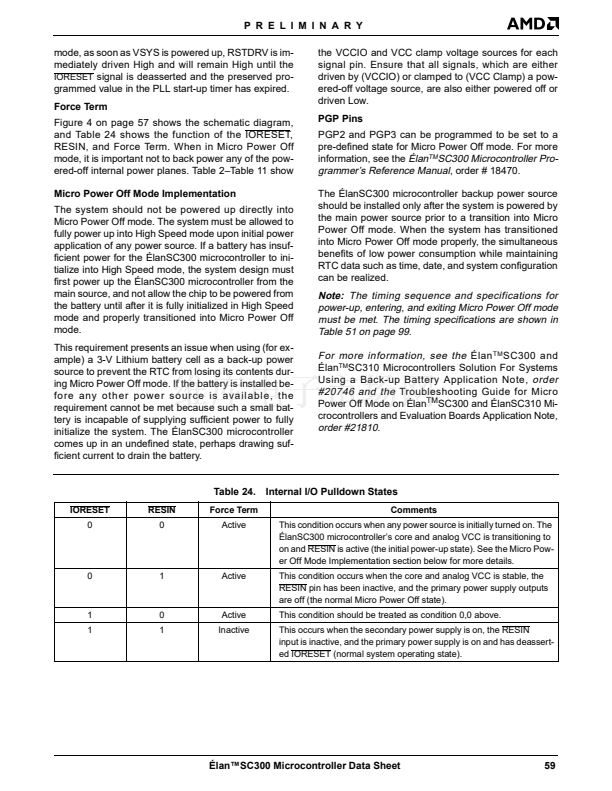 59
59
 60
60
 61
61
 62
62
 63
63
 64
64
 65
65
 66
66
 67
67
 68
68
 69
69
 70
70
 71
71
 72
72
 73
73
 74
74
 75
75
 76
76
 77
77
 78
78
 79
79
 80
80
 81
81
 82
82
 83
83
 84
84
 85
85
 86
86
 87
87
 88
88
 89
89
 90
90
 91
91
 92
92
 93
93
 94
94
 95
95
 96
96
 97
97
 98
98
 99
99
 100
100
 101
101
 102
102
 103
103
 104
104
 105
105
 106
106
 107
107
 108
108
 109
109
 110
110
 111
111
 112
112
 113
113
 114
114
 115
115
 116
116
 117
117
 118
118
 119
119
 120
120
 121
121
 122
122
 123
123
 124
124
 125
125
 126
126
 127
127
 128
128
 129
129
 130
130
 131
131
 132
132
 133
133
 134
134
 135
135
 136
136
 137
137
 138
138
 139
139
