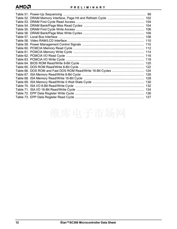
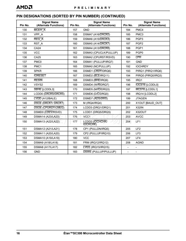
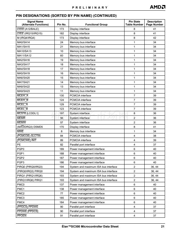
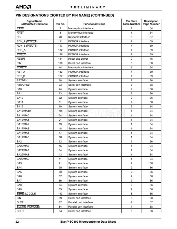
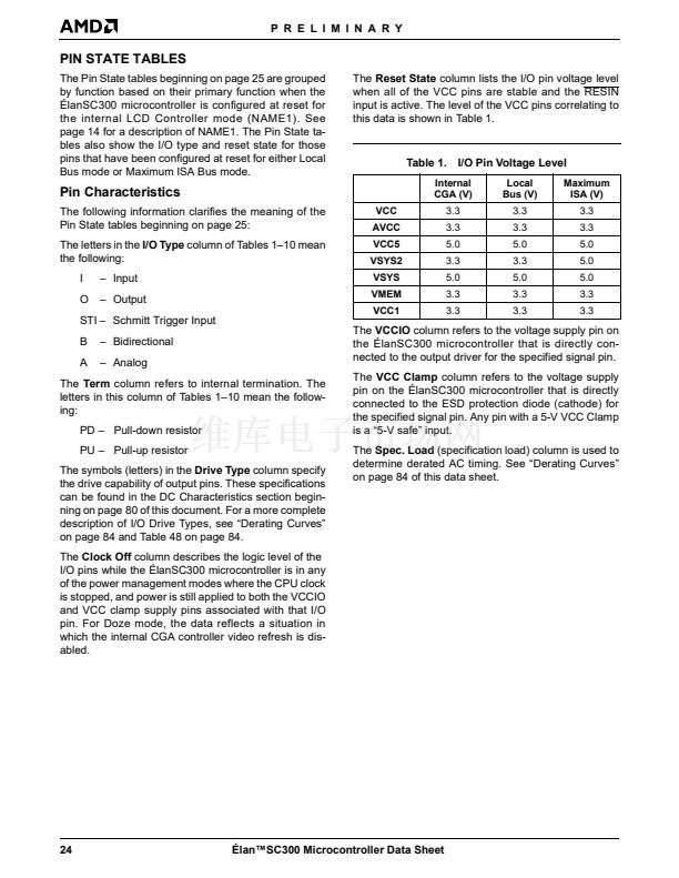
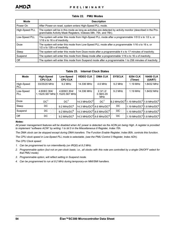
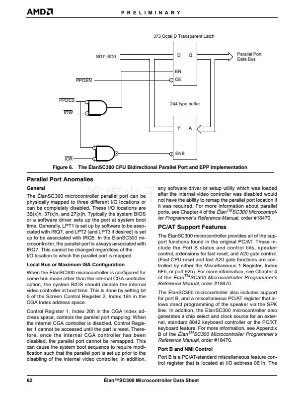
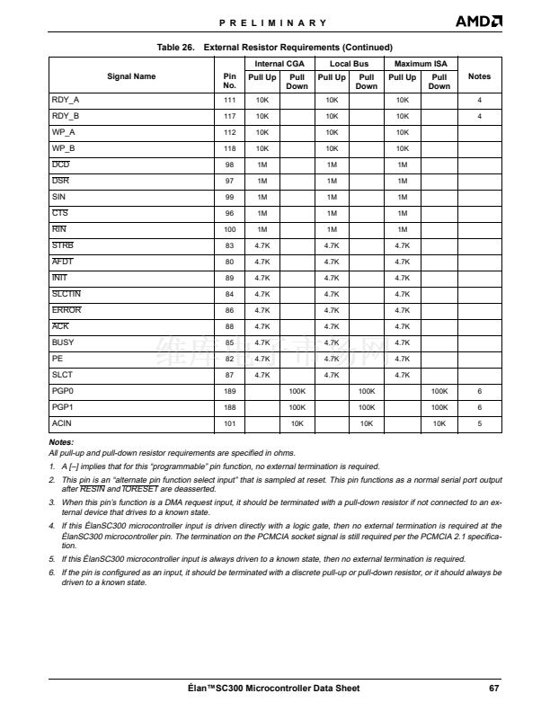
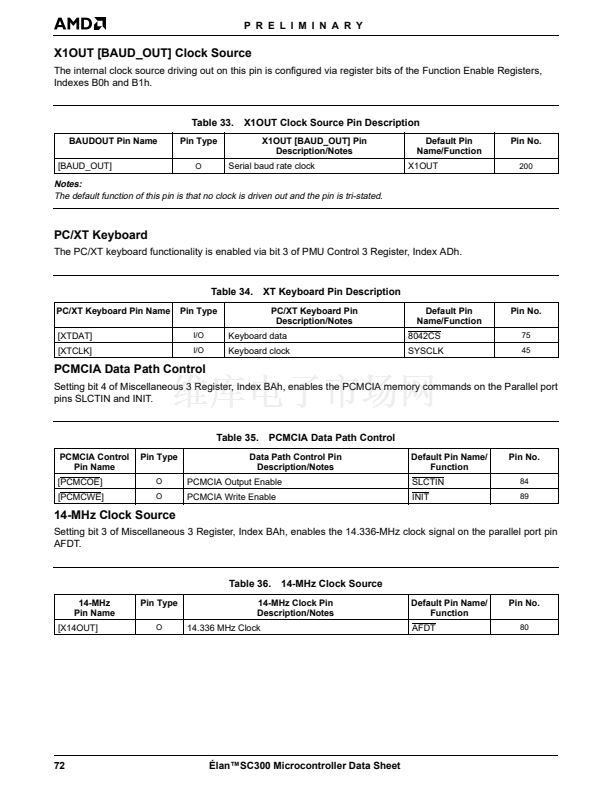
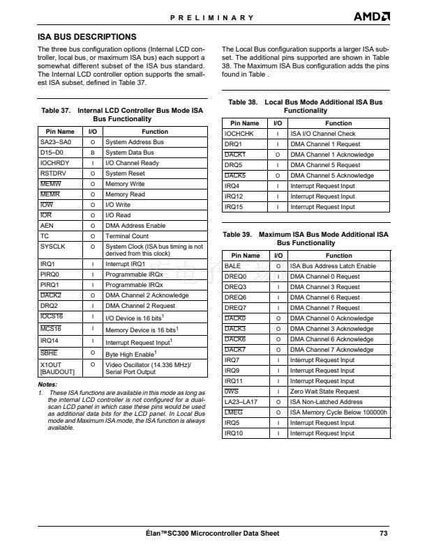
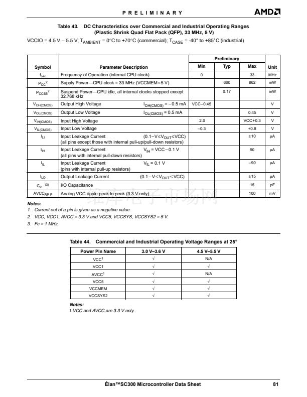
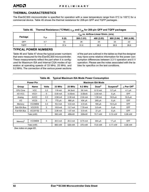
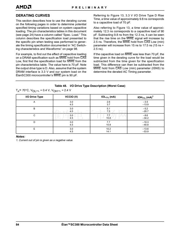
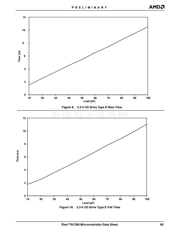
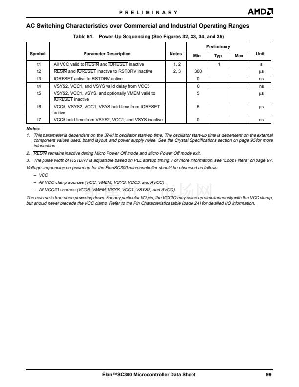
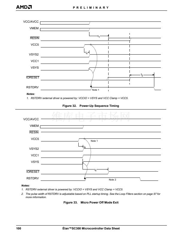
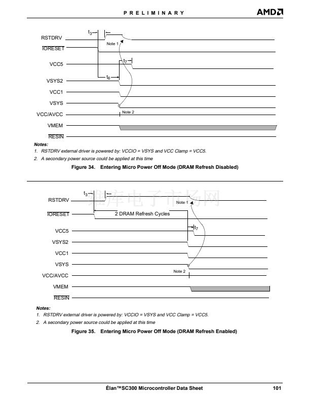
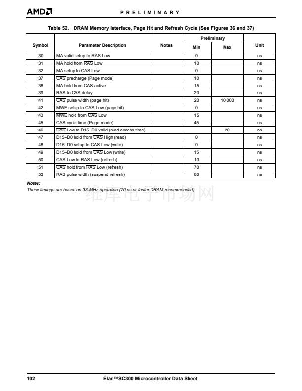
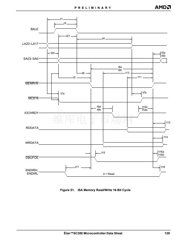
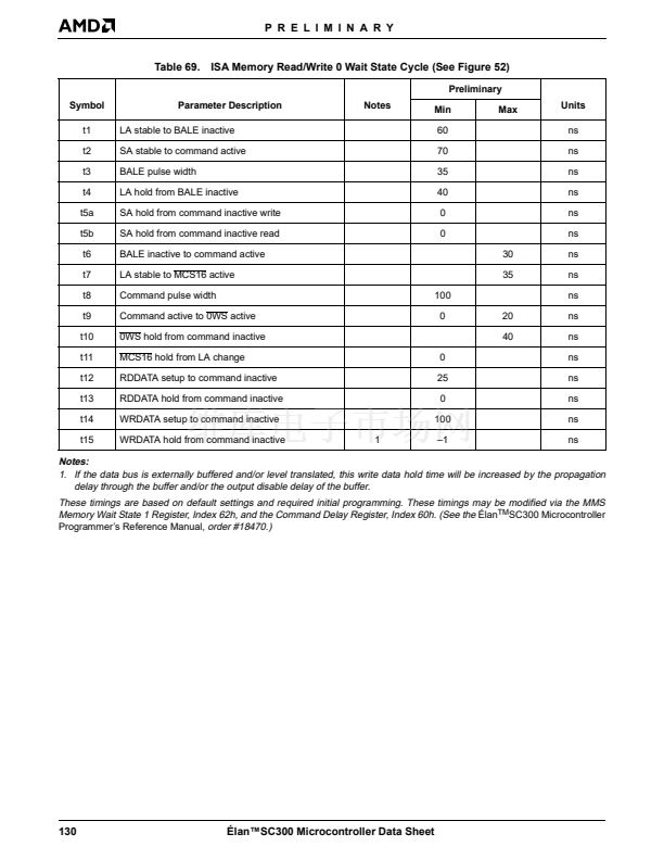
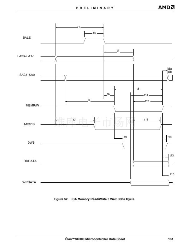
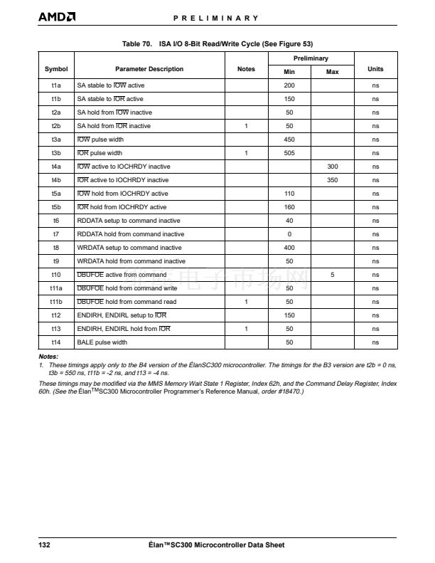
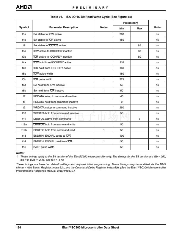
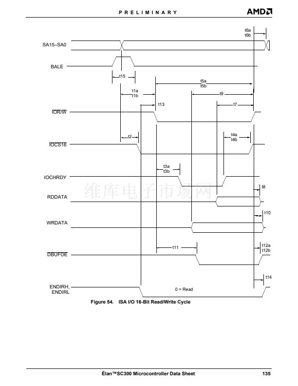
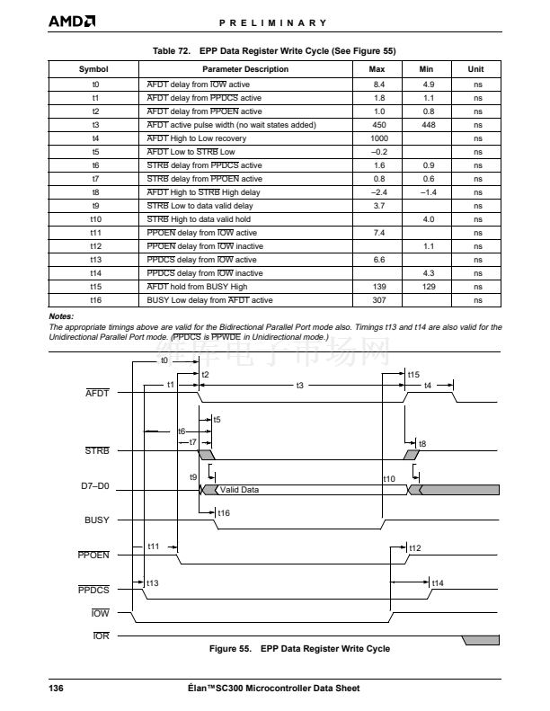
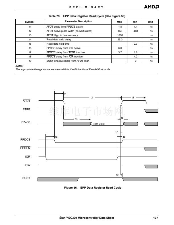
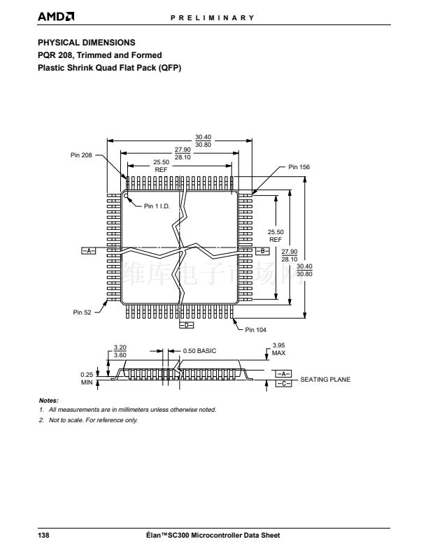
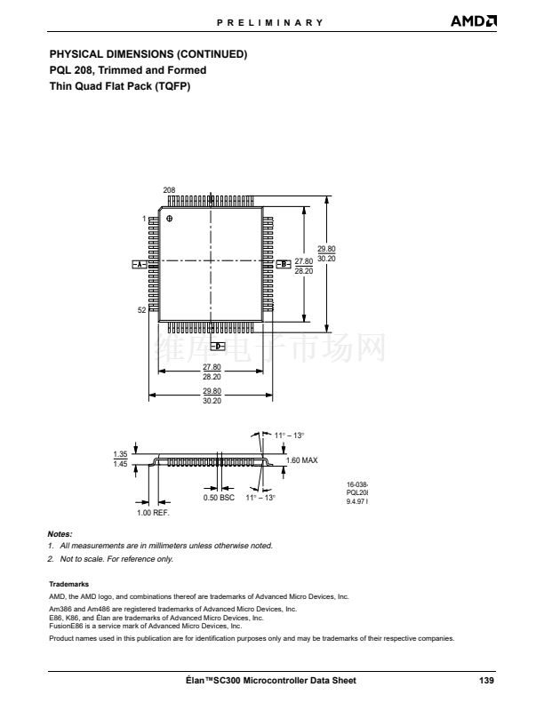
P R E L I M I N A R Y
Am386
庐
SX/SXL/SXLV Data Sheet,
order #21020 and
the
Am386
庐
DX/DXL Data Sheet,
order #21017.
Along with standard 386 architectural features, the
CPU core includes SMM. SMM and the other features
of the CPU are described in the
Am386DXLV and
Am386SXLV Microprocessors Technical Reference
Manual,
order #16944.
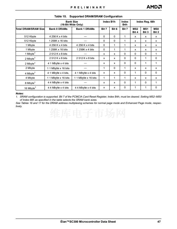
banks supporting up to 16 Mbyte of DRAM, utilizing in-
dustry standard modules. The 脡lanSC300 microcon-
troller shares the DRAM address lines MA0鈥揗A11 with
the upper system address lines SA12鈥揝A23 to reduce
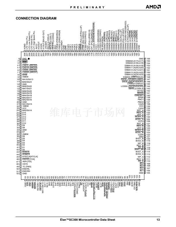
pin count. This signal sharing is shown in Table 14.
Memory Controller
The 脡lanSC300 microcontroller memory controller is a
unified control unit that supports a high-performance,
16-bit data path to DRAM or SRAM. No external mem-
ory bus buffers are required and up to 16 Mbyte in two
16-bit banks can be supported. System memory must
always be configured as 16-bits wide. For more infor-
mation about the memory controller, see Chapter 2 of
the
脡lan
TM
SC300 Microcontroller Programmer鈥檚 Refer-
ence Manual
, order #18470. The System Block Dia-
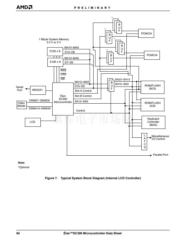
gram, Figure 7 on page 64 of this manual, shows a
typical palm-top memory configuration.
The 脡lanSC300 microcontroller鈥檚 memory controller
supports an EMS-compatible Memory Mapping Sys-
tem (MMS) with 12 page registers. This facility can be
used to provide access to ROM-based software. MMS
is also used in the PCMCIA slot support. Shadow RAM
is also supported.
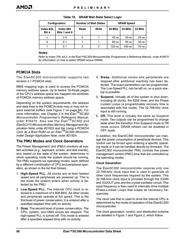
The Memory Controller supports one of three different
memory operating modes: SRAM, Page mode DRAM,
or Enhanced Page mode DRAM. Enhanced Page
mode increases DRAM access performance by effec-
tively doubling the DRAM page size in a two-bank
DRAM system by arranging the address lines such that
one page is spread across both DRAM banks. Both
DRAM modes use standard Fast Page mode DRAMs.
The memory controller operation is synchronous with
respect to the CPU. This ensures maximum perfor-
mance for all transfers to local memory. The clock
stretching implemented by the clock generation cir-
cuitry works to reduce synchronous logic power con-
sumption.
As shown in Table 13, the two DRAM operating modes
are defined by the MOD field in the Memory Configura-
tion Register, Index 66h, bit 0.
Table 14.
MA and SA Signal Pin Sharing
DRAM Memory Address
MA9鈥揗A0
MA10
MA11
System Address
SA23鈥揝A14
SA13
SA12
The 脡lanSC300 microcontroller also shares the DRAM
data bus with the system data bus on the D15鈥揇0 pins.
In a typical system, an SD bus is created with an exter-
nal x 16 bit buffer or level translator to isolate the
DRAM data bus from the rest of the system. Refer to
the Typical System Block Diagram, Figure 7 on page
64 of this data sheet. The DRAM configurations are
supported as shown in Table 11. The bank size infor-
mation in the table also applies when system memory
is configured as SRAM; however, SRAM uses a differ-
ent addressing scheme than DRAM and shares the
same address lines as the ISA bus. Chapter 2 in the
脡lan
TM
SC300 Microcontroller Programmer鈥檚 Refer-
ence Manual
, order #18470, contains more informa-
tion. Note that the configurations that use 512 Kbyte x
8 bit and 1 Mbyte x 16 bit DRAMs employ asymmetrical
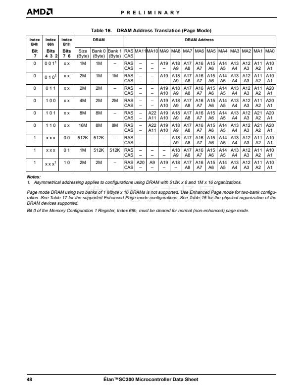
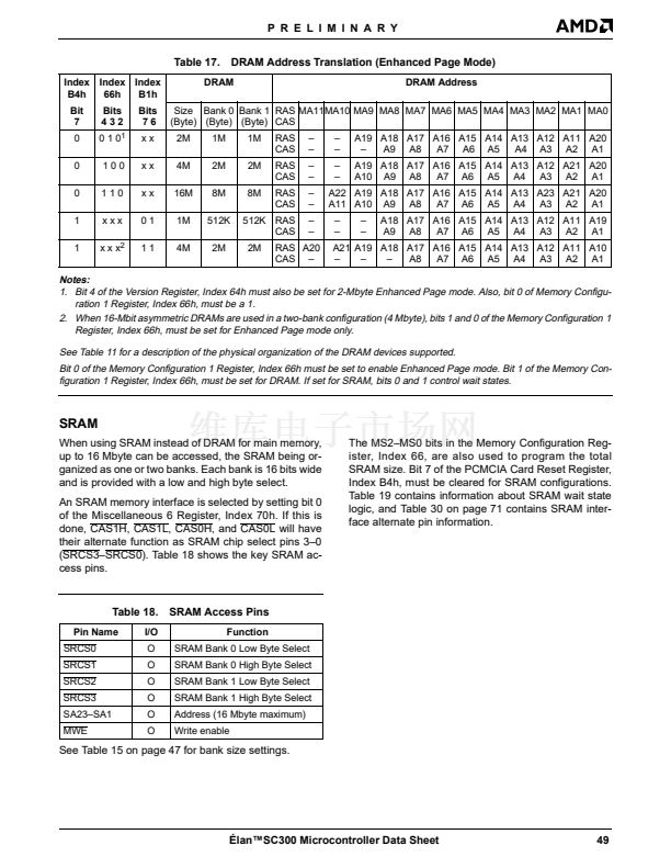
addressing. Table 16 and Table 17 show the relation-
ship of the CPU address mapped to the DRAM mem-
ory.
Table 13.
0
1
DRAM Mode Selection
Function
Page mode
Enhanced Page mode
MOD0 (Index 66h, bit 0)
The 脡lanSC300 microcontroller defaults to a DRAM in-
terface. The SRAM mode is selected via bit 0 of the
Miscellaneous 6 Register Index 70h. The memory con-
troller provides for a direct connection of two 16-bit
46
脡lan鈩C300 Microcontroller Data Sheet


 1
1
 2
2
 3
3
 4
4
 5
5
 6
6
 7
7
 8
8
 9
9
 10
10
 11
11
 12
12
 13
13
 14
14
 15
15
 16
16
 17
17
 18
18
 19
19
 20
20
 21
21
 22
22
 23
23
 24
24
 25
25
 26
26
 27
27
 28
28
 29
29
 30
30
 31
31
 32
32
 33
33
 34
34
 35
35
 36
36
 37
37
 38
38
 39
39
 40
40
 41
41
 42
42
 43
43
 44
44
 45
45
 46
46
 47
47
 48
48
 49
49
 50
50
 51
51
 52
52
 53
53
 54
54
 55
55
 56
56
 57
57
 58
58
 59
59
 60
60
 61
61
 62
62
 63
63
 64
64
 65
65
 66
66
 67
67
 68
68
 69
69
 70
70
 71
71
 72
72
 73
73
 74
74
 75
75
 76
76
 77
77
 78
78
 79
79
 80
80
 81
81
 82
82
 83
83
 84
84
 85
85
 86
86
 87
87
 88
88
 89
89
 90
90
 91
91
 92
92
 93
93
 94
94
 95
95
 96
96
 97
97
 98
98
 99
99
 100
100
 101
101
 102
102
 103
103
 104
104
 105
105
 106
106
 107
107
 108
108
 109
109
 110
110
 111
111
 112
112
 113
113
 114
114
 115
115
 116
116
 117
117
 118
118
 119
119
 120
120
 121
121
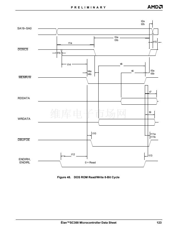
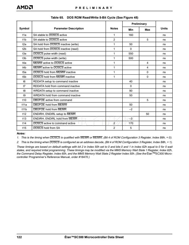 122
122
 123
123
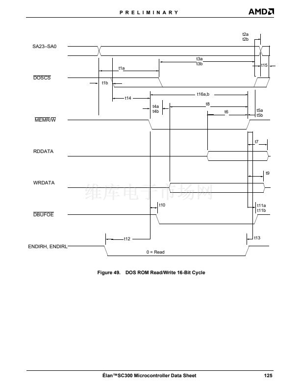
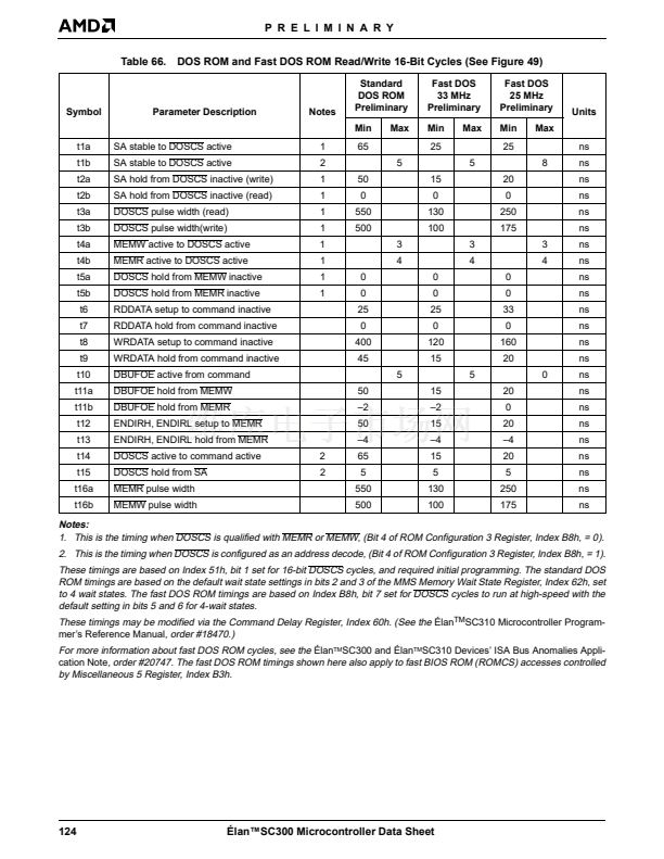 124
124
 125
125
 126
126
 127
127
 128
128
 129
129
 130
130
 131
131
 132
132
 133
133
 134
134
 135
135
 136
136
 137
137
 138
138
 139
139
