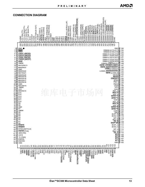
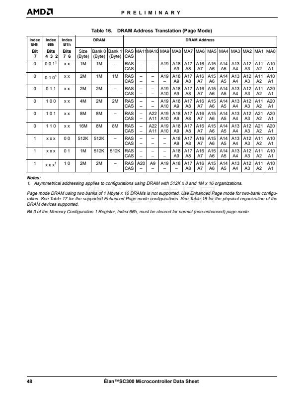
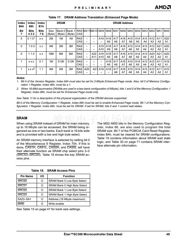
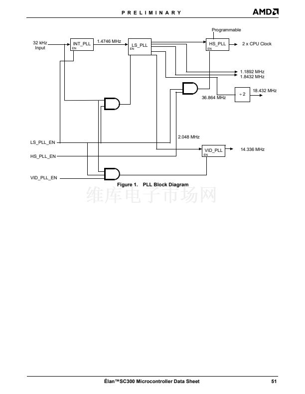
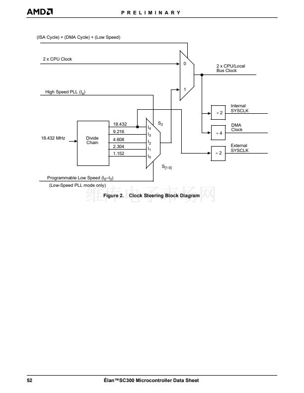
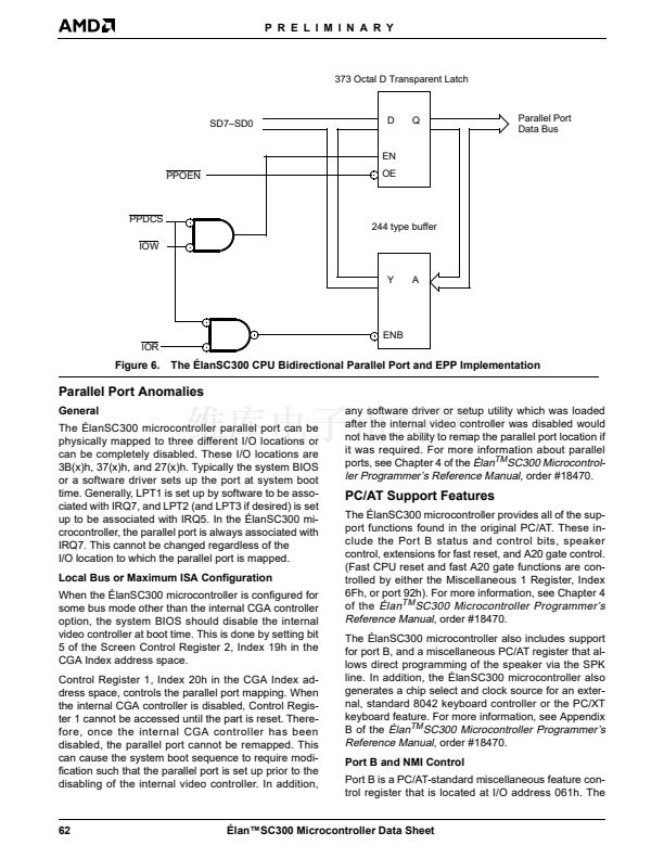
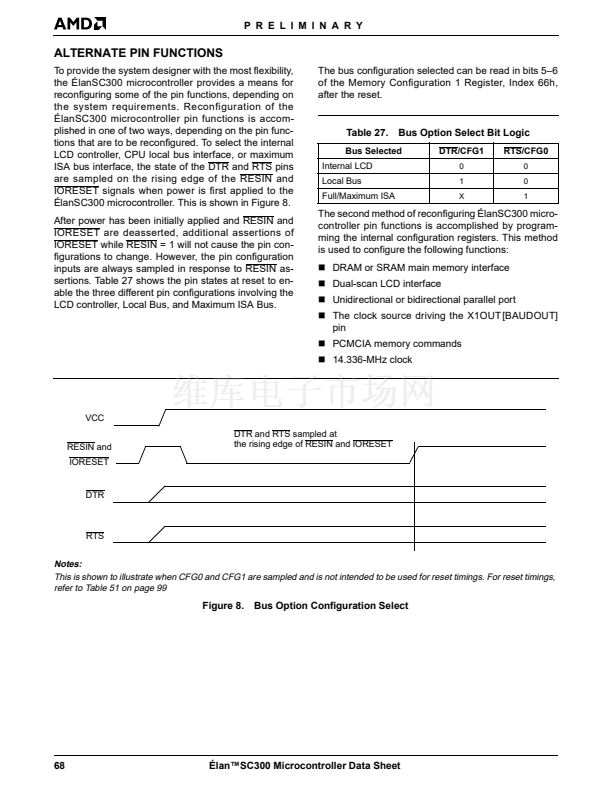
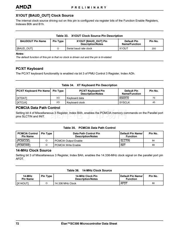
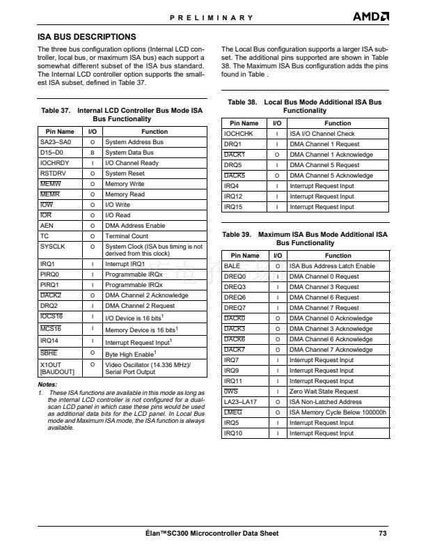
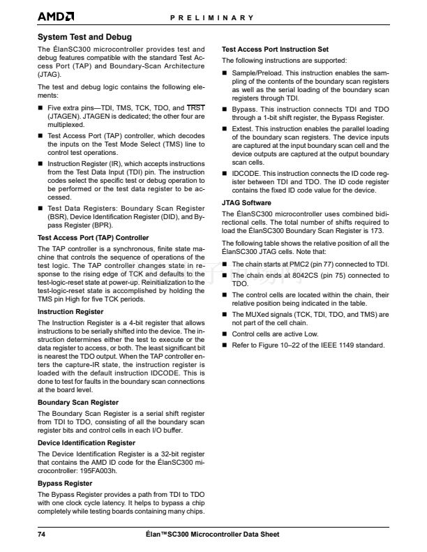
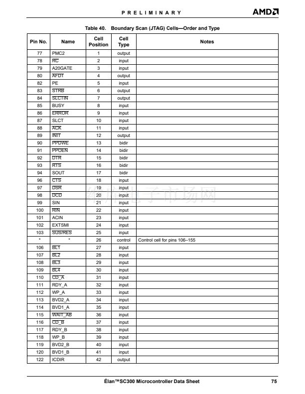
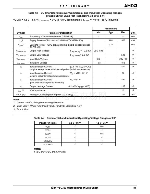
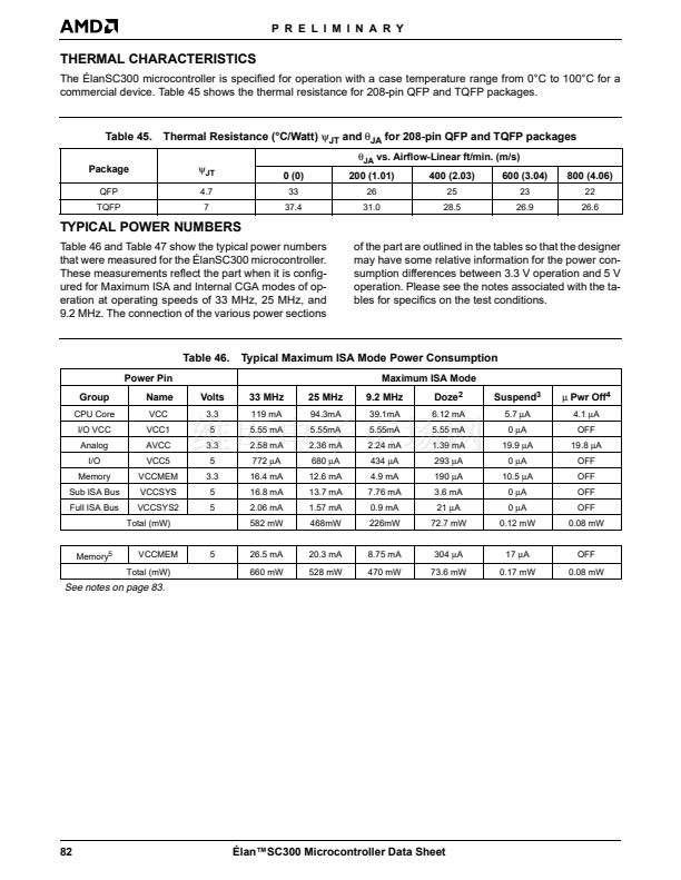
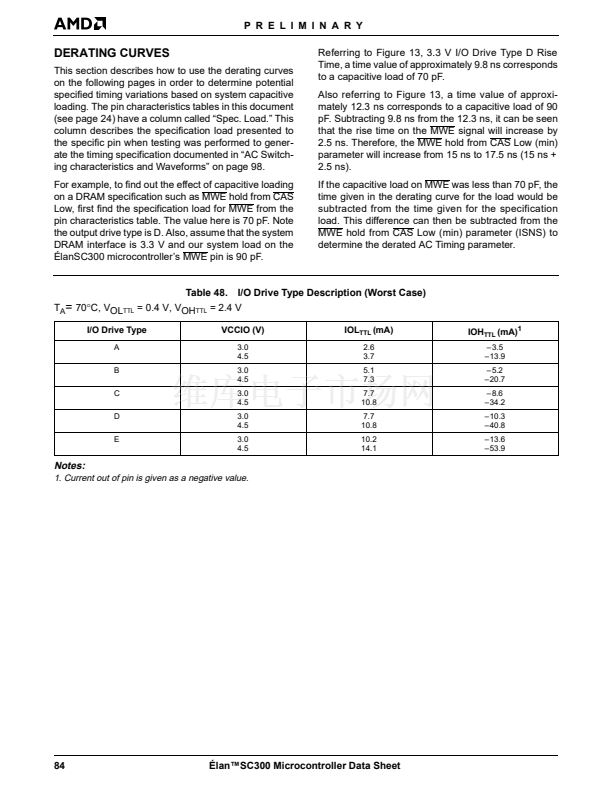
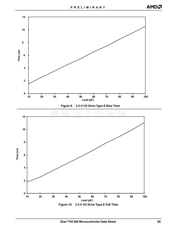
鈥?/div>
A8
A7 A6 A5 A4 A3 A2 A1
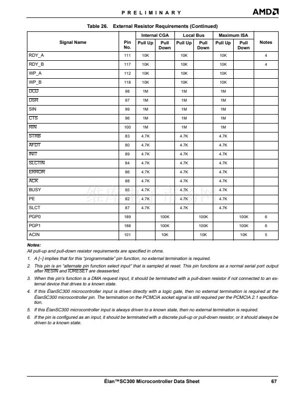
Notes:
1. Bit 4 of the Version Register, Index 64h must also be set for 2-Mbyte Enhanced Page mode. Also, bit 0 of Memory Configu-
ration 1 Register, Index 66h, must be a 1.
2. When 16-Mbit asymmetric DRAMs are used in a two-bank configuration (4 Mbyte), bits 1 and 0 of the Memory Configuration 1
Register, Index 66h, must be set for Enhanced Page mode only.
See Table 11 for a description of the physical organization of the DRAM devices supported.
Bit 0 of the Memory Configuration 1 Register, Index 66h must be set to enable Enhanced Page mode. Bit 1 of the Memory Con-
figuration 1 Register, Index 66h, must be set for DRAM. If set for SRAM, bits 0 and 1 control wait states.
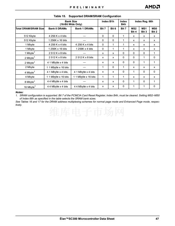
SRAM
When using SRAM instead of DRAM for main memory,
up to 16 Mbyte can be accessed, the SRAM being or-
ganized as one or two banks. Each bank is 16 bits wide
and is provided with a low and high byte select.
An SRAM memory interface is selected by setting bit 0
of the Miscellaneous 6 Register, Index 70h. If this is
done, CAS1H, CAS1L, CAS0H, and CAS0L will have
their alternate function as SRAM chip select pins 3鈥?
(SRCS3鈥揝RCS0). Table 18 shows the key SRAM ac-
cess pins.
The MS2鈥揗S0 bits in the Memory Configuration Reg-
ister, Index 66, are also used to program the total
SRAM size. Bit 7 of the PCMCIA Card Reset Register,
Index B4h, must be cleared for SRAM configurations.
Table 19 contains information about SRAM wait state
logic, and Table 30 on page 71 contains SRAM inter-
face alternate pin information.
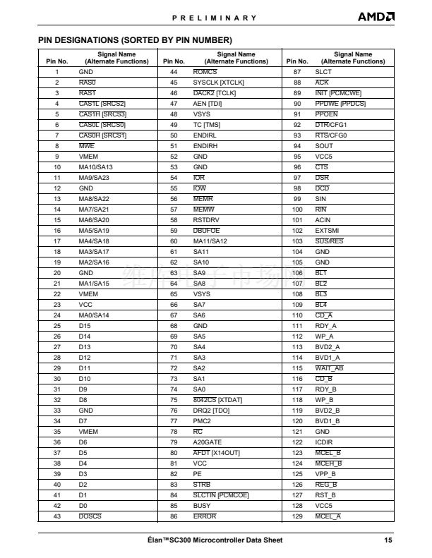
Table 18. SRAM Access Pins
Pin Name
SRCS0
SRCS1
SRCS2
SRCS3
SA23鈥揝A1
MWE
I/O
O
O
O
O
O
O
Function
SRAM Bank 0 Low Byte Select
SRAM Bank 0 High Byte Select
SRAM Bank 1 Low Byte Select
SRAM Bank 1 High Byte Select
Address (16 Mbyte maximum)
Write enable
See Table 15 on page 47 for bank size settings.
脡lan鈩C300 Microcontroller Data Sheet
49


 1
1
 2
2
 3
3
 4
4
 5
5
 6
6
 7
7
 8
8
 9
9
 10
10
 11
11
 12
12
 13
13
 14
14
 15
15
 16
16
 17
17
 18
18
 19
19
 20
20
 21
21
 22
22
 23
23
 24
24
 25
25
 26
26
 27
27
 28
28
 29
29
 30
30
 31
31
 32
32
 33
33
 34
34
 35
35
 36
36
 37
37
 38
38
 39
39
 40
40
 41
41
 42
42
 43
43
 44
44
 45
45
 46
46
 47
47
 48
48
 49
49
 50
50
 51
51
 52
52
 53
53
 54
54
 55
55
 56
56
 57
57
 58
58
 59
59
 60
60
 61
61
 62
62
 63
63
 64
64
 65
65
 66
66
 67
67
 68
68
 69
69
 70
70
 71
71
 72
72
 73
73
 74
74
 75
75
 76
76
 77
77
 78
78
 79
79
 80
80
 81
81
 82
82
 83
83
 84
84
 85
85
 86
86
 87
87
 88
88
 89
89
 90
90
 91
91
 92
92
 93
93
 94
94
 95
95
 96
96
 97
97
 98
98
 99
99
 100
100
 101
101
 102
102
 103
103
 104
104
 105
105
 106
106
 107
107
 108
108
 109
109
 110
110
 111
111
 112
112
 113
113
 114
114
 115
115
 116
116
 117
117
 118
118
 119
119
 120
120
 121
121
 122
122
 123
123
 124
124
 125
125
 126
126
 127
127
 128
128
 129
129
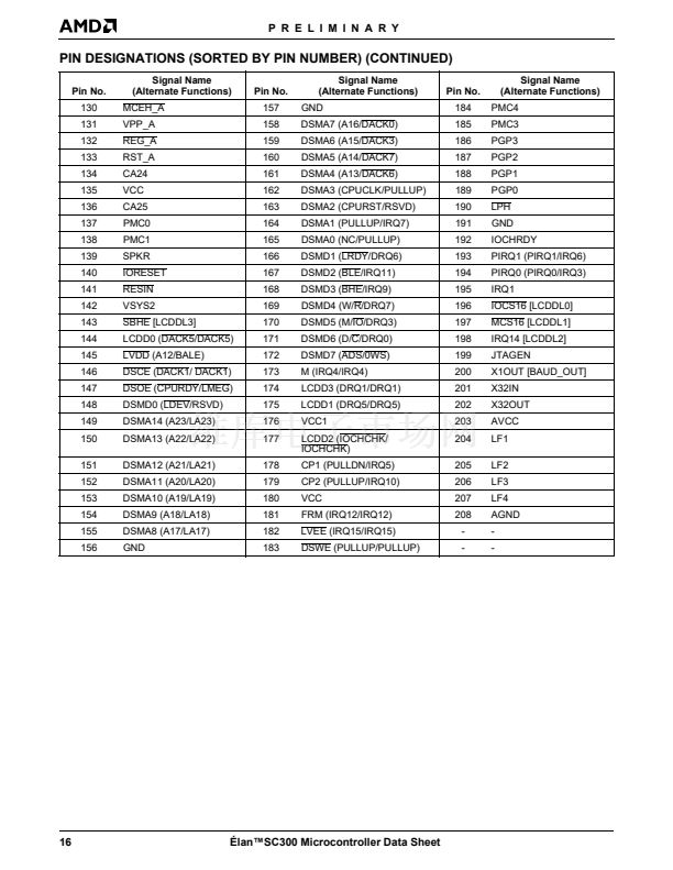
 130
130
 131
131
 132
132
 133
133
 134
134
 135
135
 136
136
 137
137
 138
138
 139
139
