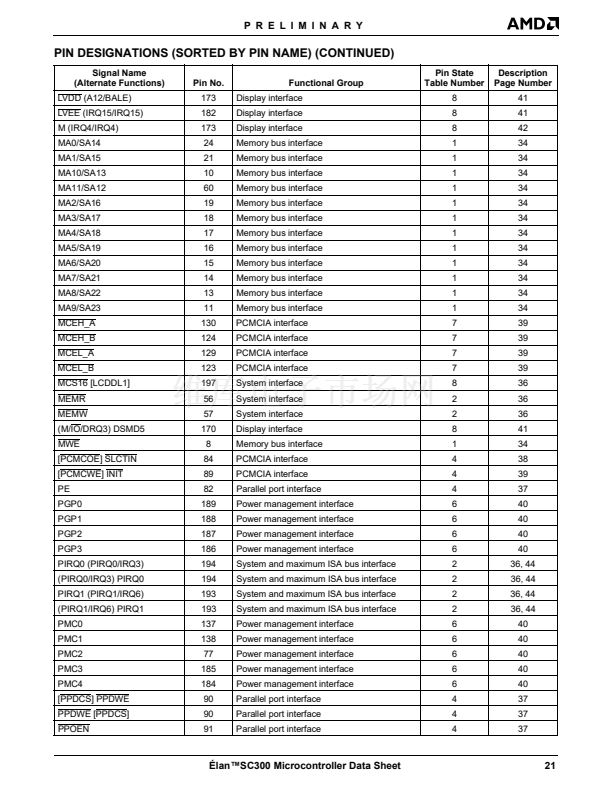
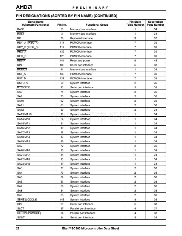
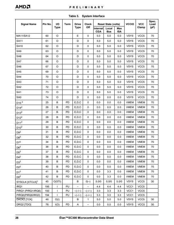
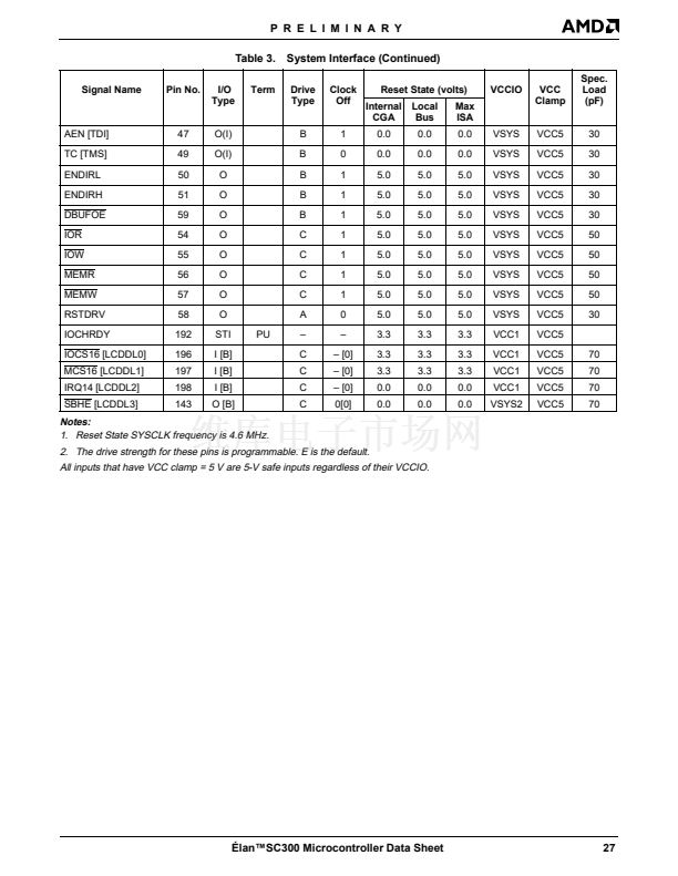
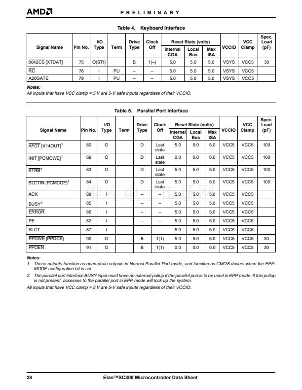
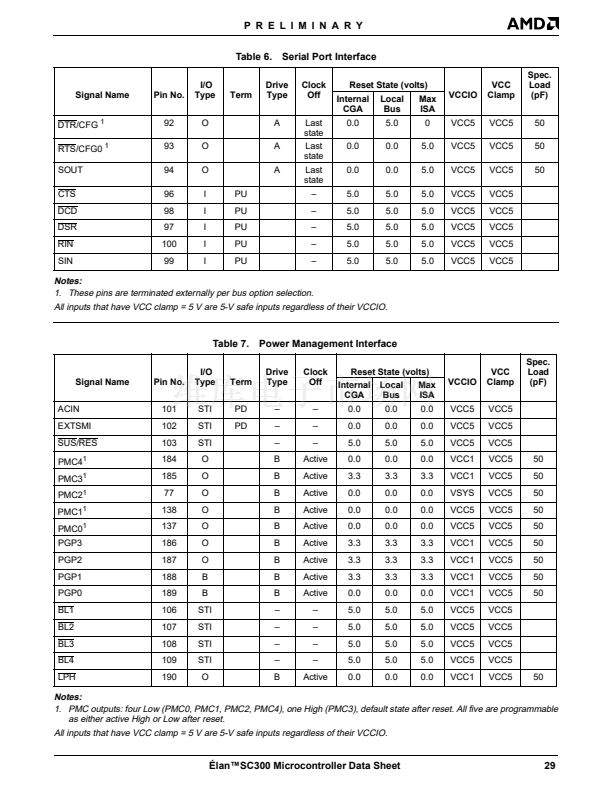
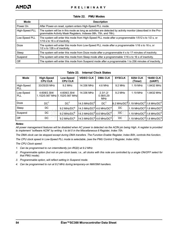
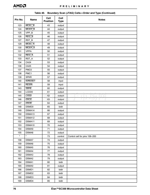
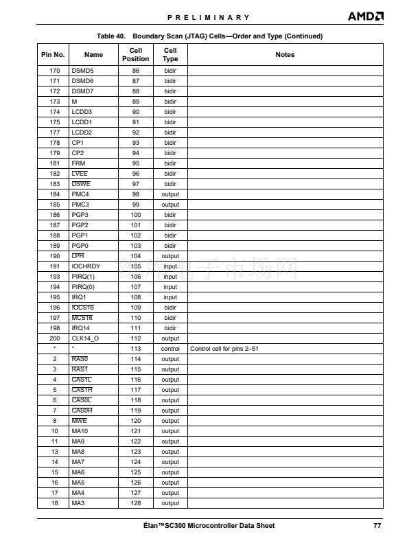
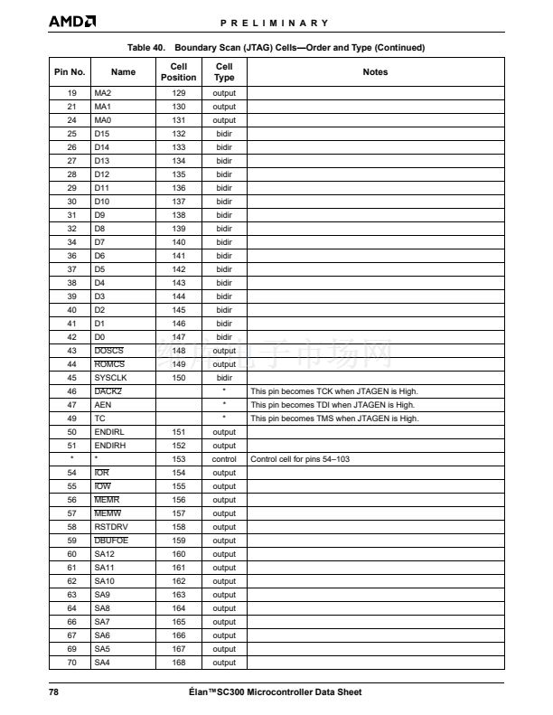
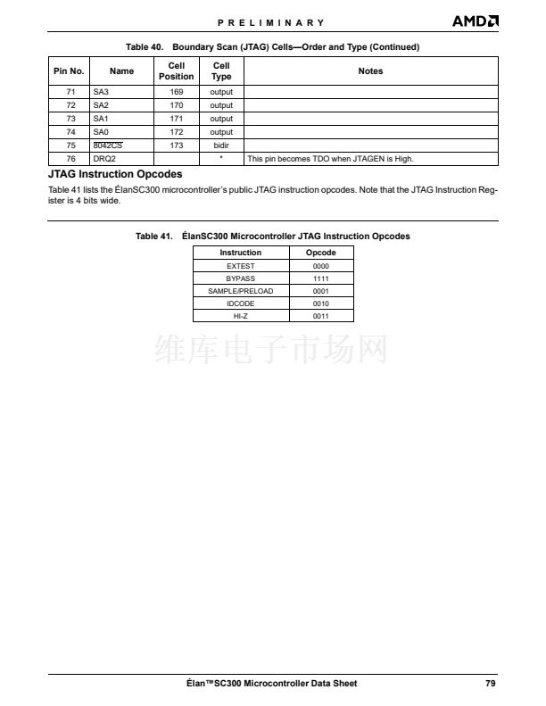
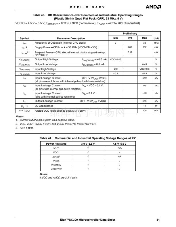
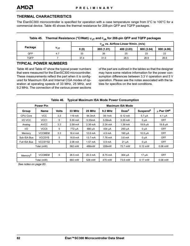
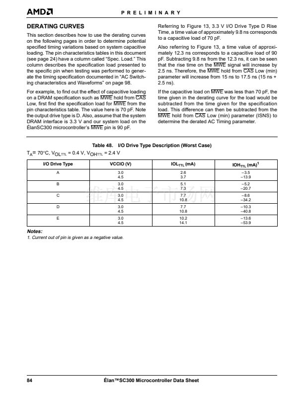
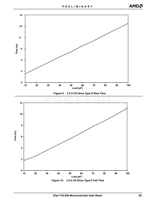
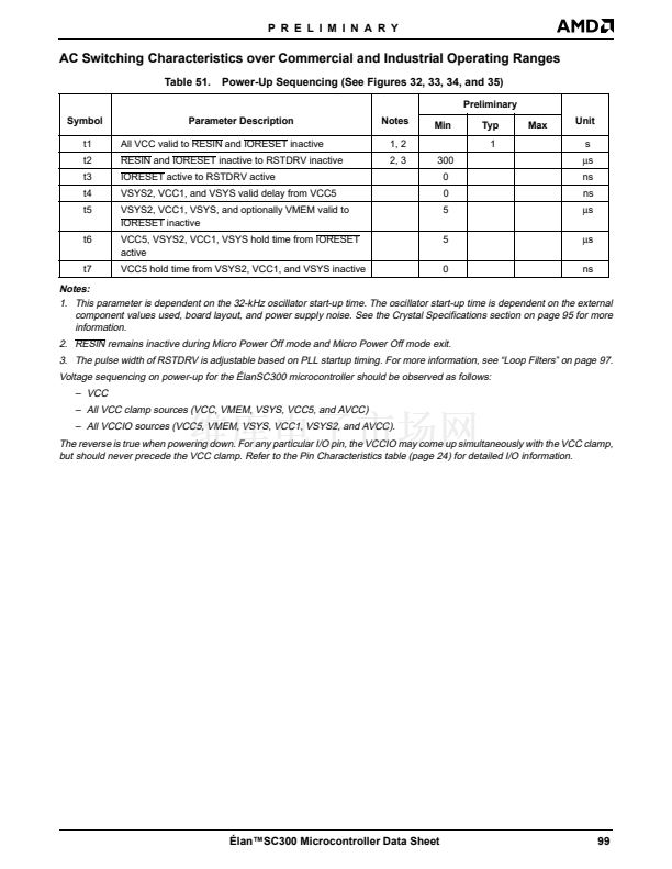
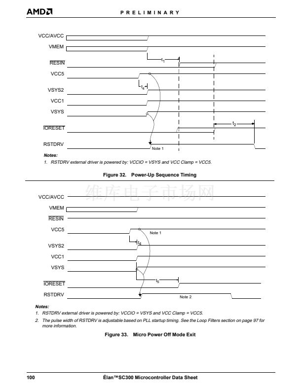
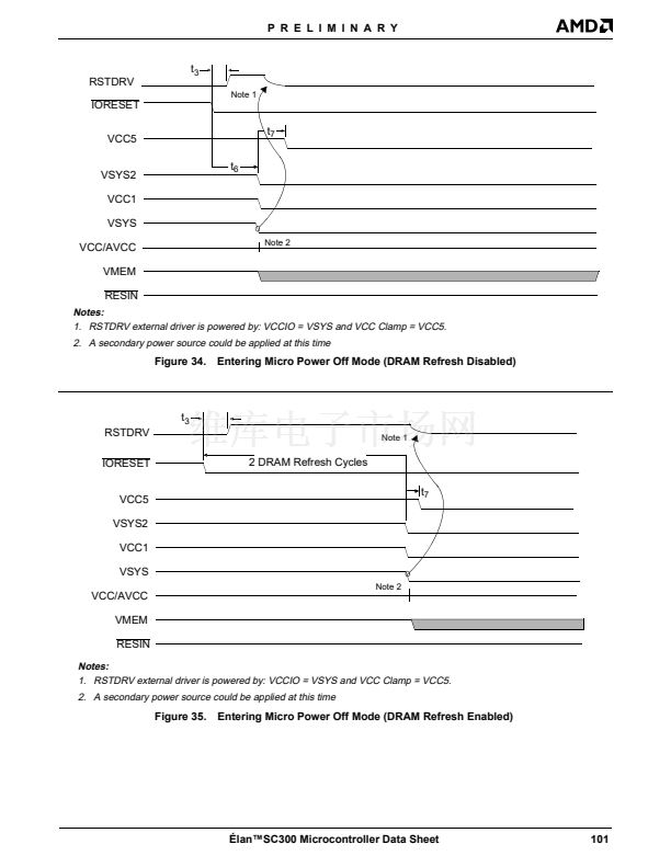
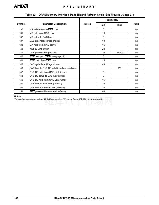
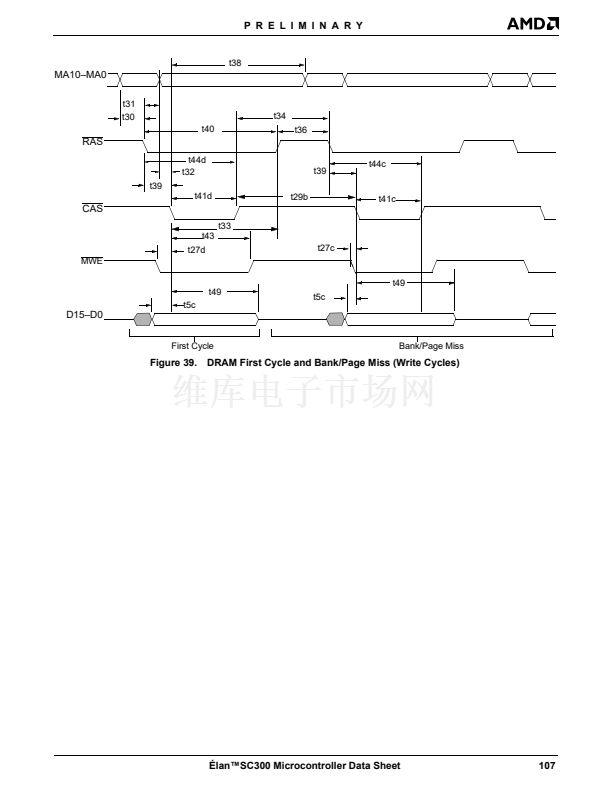
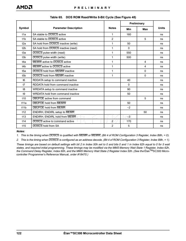
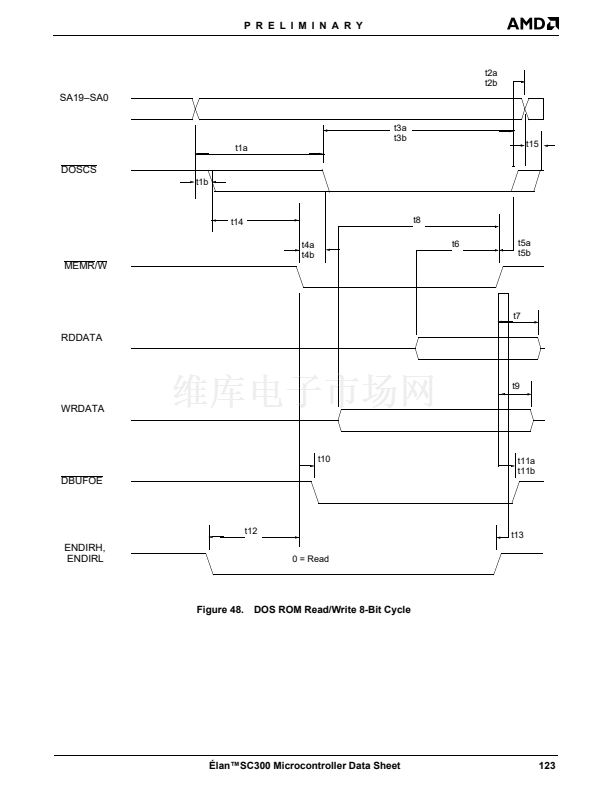
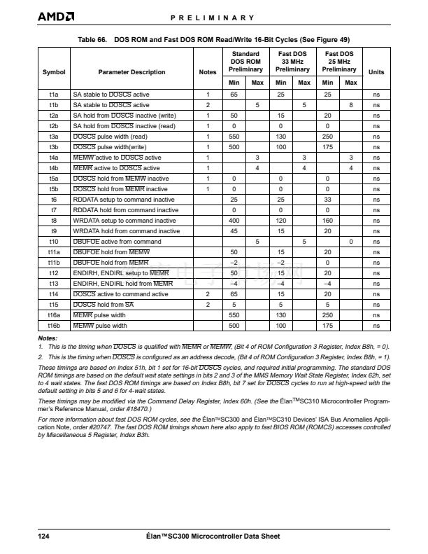
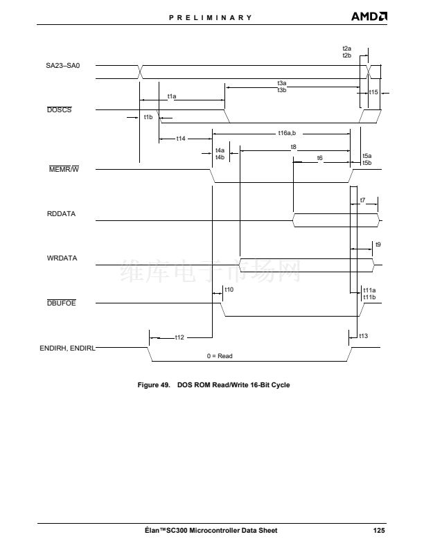
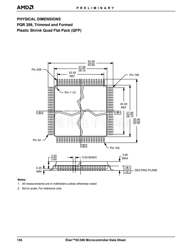
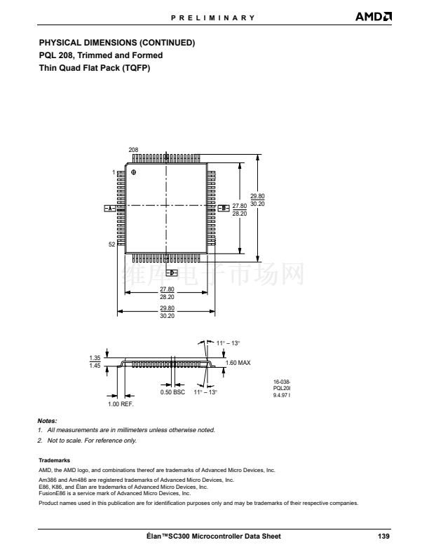
P R E L I M I N A R Y
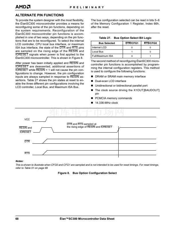
ALTERNATE PIN FUNCTIONS SELECTED VIA FIRMWARE
The following tables contain brief descriptions of the alternate pin functions/names and the pin names of the default
function that the alternate function replaces. These alternate functions are selected via system firmware only.
SRAM Interface
This alternate function is configured by setting bit 0 of the Miscellaneous 6 Register, Index 70h.
Table 30.
SRAM Pin Name
[SRCS0]
[SRCS1]
[SRCS2]
[SRCS3]
Pin Type
O
O
O
O
SRAM Interface
Default Pin
Name/Function
CAS0L
CAS0H
CAS1L
CAS1H
Pin No.
6
7
4
5
SRAM Interface Pin
Description/Notes
SRAM Bank 0 Chip Select. Low Byte
SRAM Bank 0 Chip Select. High Byte
SRAM Bank 1 Chip Select. Low Byte
SRAM Bank 1 Chip Select. High Byte
Dual-Scan LCD Data Bus
This alternate function is configured via selecting a dual-scan LCD Panel mode in the CGA index address space at
Index 18h.
Table 31.
Dual-Scan Pin Name
[LCDDL0]
[LCDDL1]
[LCDDL2]
[LCDDL3]
Pin Type
O
O
O
O
Dual-Scan LCD Data Bus
Default Pin
Name/Function
IOCS16
MCS16
IRQ14
SBHE
Pin No.
196
197
198
143
Dual-Scan LCD Data-Bus Pin
Description/Notes
Dual screen data bit
Dual screen data bit
Dual screen data bit
Dual screen data bit
Notes:
In the dual-scan LCD configuration, IOCS16 and MCS16 are internally forced inactive.
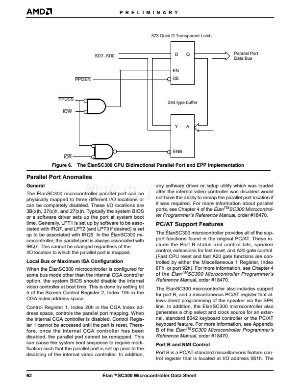
Unidirectional/Bidirectional Parallel Port
This alternate function is configured via selecting either the Normal Bidirectional mode configuration or the EPP
mode configuration for the parallel port in the Function Enable 1 Register, Index B0h.
Table 32.
Bidirectional Pin Pin Type
Name
[PPDCS]
O
Bidirectional Parallel Port Pin Description
Bidirectional Parallel Port Pin
Description/Notes
Default Pin
Name/Function
PPDWE
Pin No.
90
Parallel Port data register address decode
脡lan鈩C300 Microcontroller Data Sheet
71


 1
1
 2
2
 3
3
 4
4
 5
5
 6
6
 7
7
 8
8
 9
9
 10
10
 11
11
 12
12
 13
13
 14
14
 15
15
 16
16
 17
17
 18
18
 19
19
 20
20
 21
21
 22
22
 23
23
 24
24
 25
25
 26
26
 27
27
 28
28
 29
29
 30
30
 31
31
 32
32
 33
33
 34
34
 35
35
 36
36
 37
37
 38
38
 39
39
 40
40
 41
41
 42
42
 43
43
 44
44
 45
45
 46
46
 47
47
 48
48
 49
49
 50
50
 51
51
 52
52
 53
53
 54
54
 55
55
 56
56
 57
57
 58
58
 59
59
 60
60
 61
61
 62
62
 63
63
 64
64
 65
65
 66
66
 67
67
 68
68
 69
69
 70
70
 71
71
 72
72
 73
73
 74
74
 75
75
 76
76
 77
77
 78
78
 79
79
 80
80
 81
81
 82
82
 83
83
 84
84
 85
85
 86
86
 87
87
 88
88
 89
89
 90
90
 91
91
 92
92
 93
93
 94
94
 95
95
 96
96
 97
97
 98
98
 99
99
 100
100
 101
101
 102
102
 103
103
 104
104
 105
105
 106
106
 107
107
 108
108
 109
109
 110
110
 111
111
 112
112
 113
113
 114
114
 115
115
 116
116
 117
117
 118
118
 119
119
 120
120
 121
121
 122
122
 123
123
 124
124
 125
125
 126
126
 127
127
 128
128
 129
129
 130
130
 131
131
 132
132
 133
133
 134
134
 135
135
 136
136
 137
137
 138
138
 139
139
