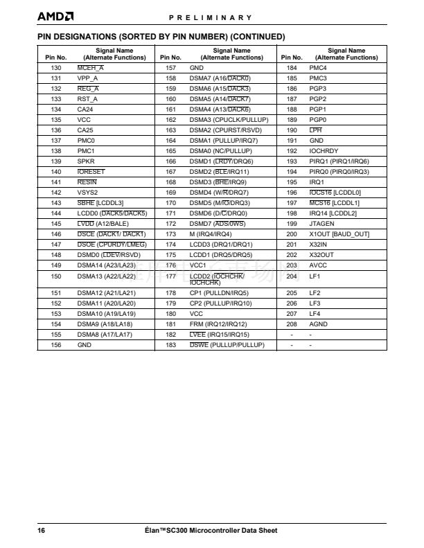
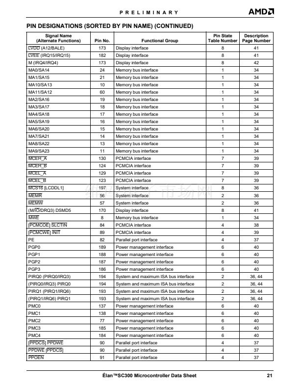
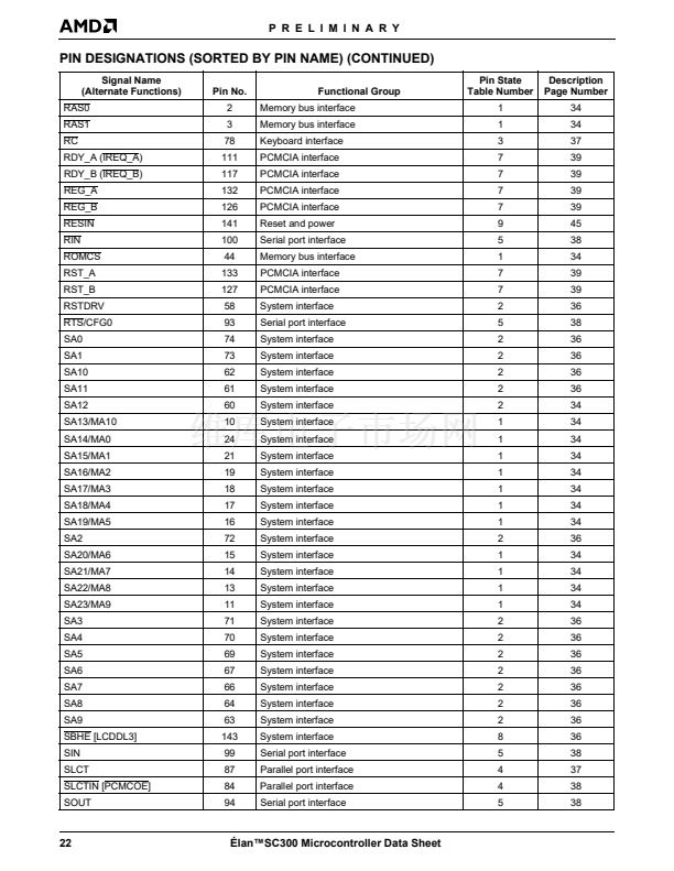
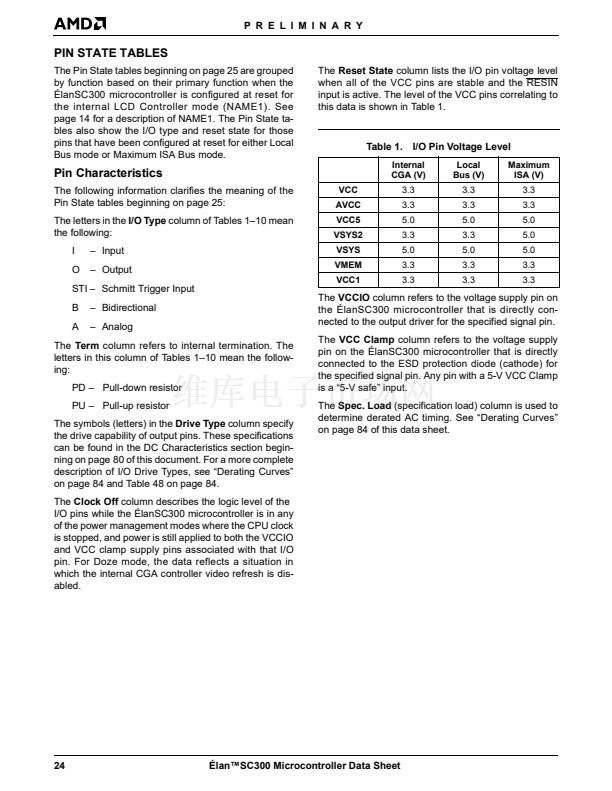
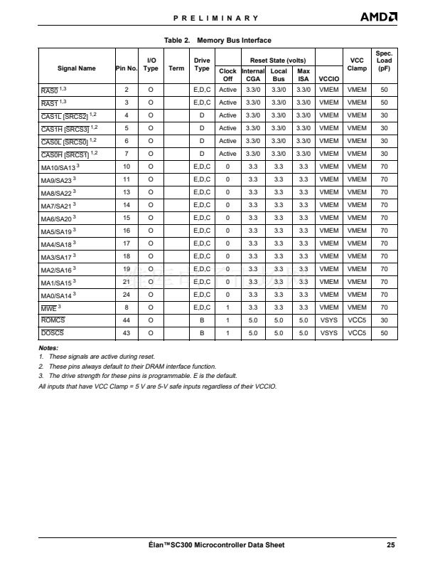
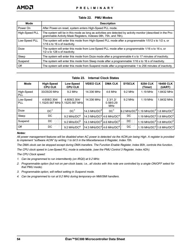
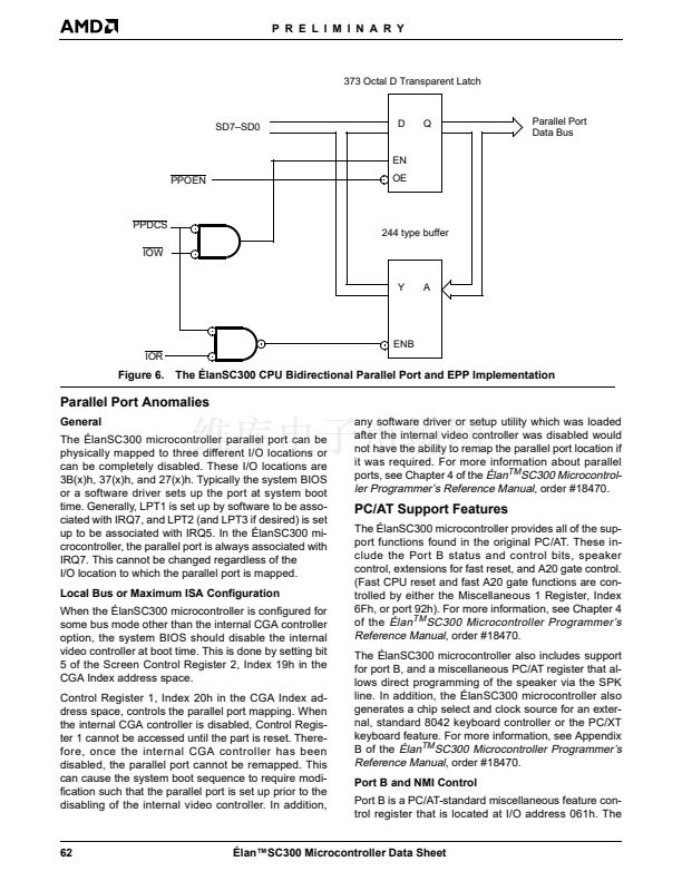
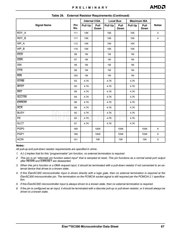
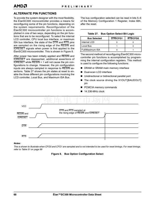
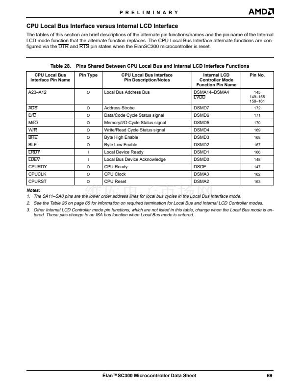
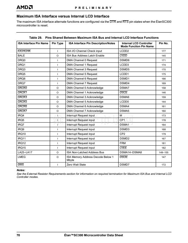
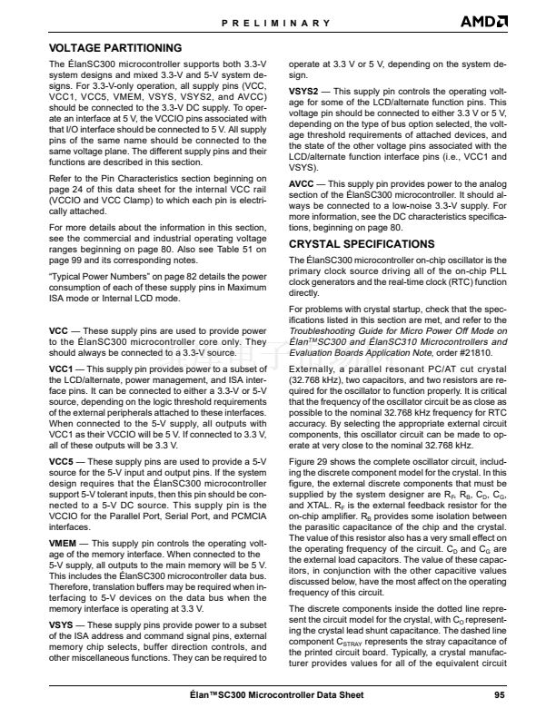
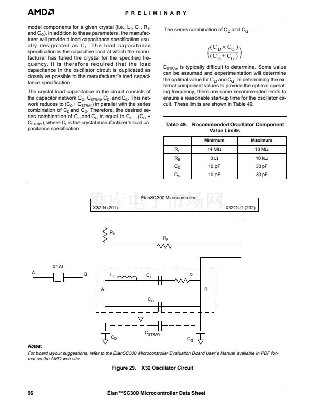
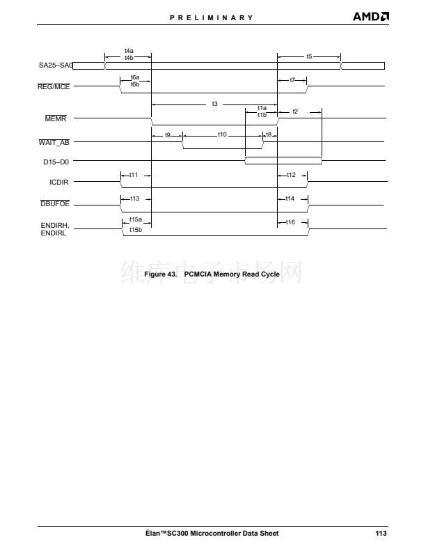
P R E L I M I N A R Y
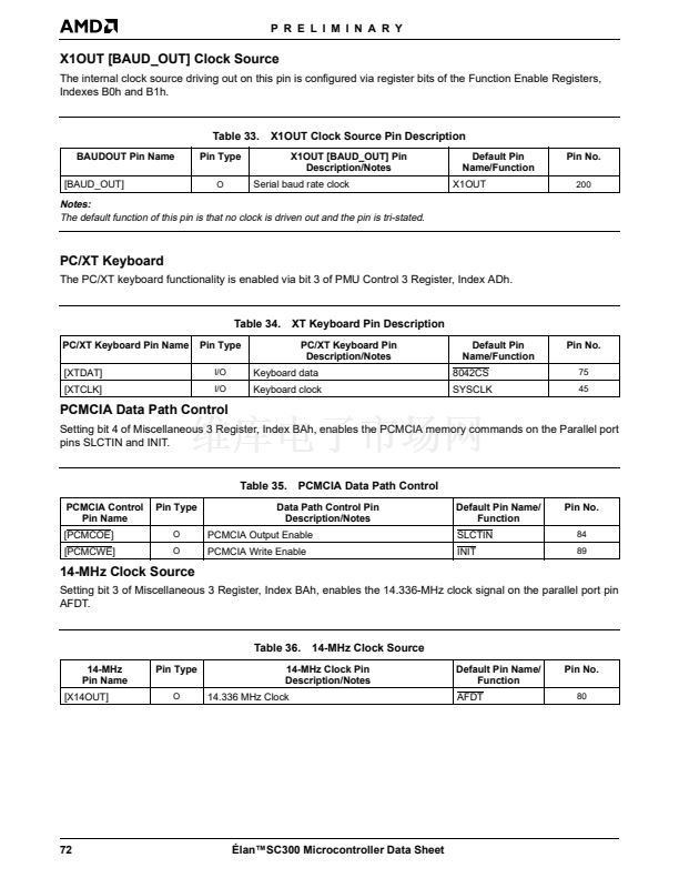
X1OUT [BAUD_OUT] Clock Source
The internal clock source driving out on this pin is configured via register bits of the Function Enable Registers,
Indexes B0h and B1h.
Table 33.
BAUDOUT Pin Name
[BAUD_OUT]
Pin Type
O
X1OUT Clock Source Pin Description
X1OUT [BAUD_OUT] Pin
Description/Notes
Default Pin
Name/Function
X1OUT
Pin No.
200
Serial baud rate clock
Notes:
The default function of this pin is that no clock is driven out and the pin is tri-stated.
PC/XT Keyboard
The PC/XT keyboard functionality is enabled via bit 3 of PMU Control 3 Register, Index ADh.
Table 34.
PC/XT Keyboard Pin Name
[XTDAT]
[XTCLK]
Pin Type
I/O
I/O
XT Keyboard Pin Description
PC/XT Keyboard Pin
Description/Notes
Default Pin
Name/Function
8042CS
SYSCLK
Pin No.
75
45
Keyboard data
Keyboard clock
PCMCIA Data Path Control
Setting bit 4 of Miscellaneous 3 Register, Index BAh, enables the PCMCIA memory commands on the Parallel port
pins SLCTIN and INIT.
Table 35. PCMCIA Data Path Control
PCMCIA Control
Pin Name
[PCMCOE]
[PCMCWE]
Pin Type
O
O
Data Path Control Pin
Description/Notes
PCMCIA Output Enable
PCMCIA Write Enable
Default Pin Name/
Function
SLCTIN
INIT
Pin No.
84
89
14-MHz Clock Source
Setting bit 3 of Miscellaneous 3 Register, Index BAh, enables the 14.336-MHz clock signal on the parallel port pin
AFDT.
Table 36. 14-MHz Clock Source
14-MHz
Pin Name
[X14OUT]
Pin Type
O
14-MHz Clock Pin
Description/Notes
14.336 MHz Clock
Default Pin Name/
Function
AFDT
Pin No.
80
72
脡lan鈩C300 Microcontroller Data Sheet


 1
1
 2
2
 3
3
 4
4
 5
5
 6
6
 7
7
 8
8
 9
9
 10
10
 11
11
 12
12
 13
13
 14
14
 15
15
 16
16
 17
17
 18
18
 19
19
 20
20
 21
21
 22
22
 23
23
 24
24
 25
25
 26
26
 27
27
 28
28
 29
29
 30
30
 31
31
 32
32
 33
33
 34
34
 35
35
 36
36
 37
37
 38
38
 39
39
 40
40
 41
41
 42
42
 43
43
 44
44
 45
45
 46
46
 47
47
 48
48
 49
49
 50
50
 51
51
 52
52
 53
53
 54
54
 55
55
 56
56
 57
57
 58
58
 59
59
 60
60
 61
61
 62
62
 63
63
 64
64
 65
65
 66
66
 67
67
 68
68
 69
69
 70
70
 71
71
 72
72
 73
73
 74
74
 75
75
 76
76
 77
77
 78
78
 79
79
 80
80
 81
81
 82
82
 83
83
 84
84
 85
85
 86
86
 87
87
 88
88
 89
89
 90
90
 91
91
 92
92
 93
93
 94
94
 95
95
 96
96
 97
97
 98
98
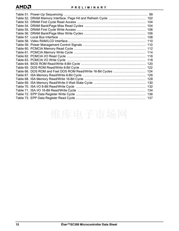
 99
99
 100
100
 101
101
 102
102
 103
103
 104
104
 105
105
 106
106
 107
107
 108
108
 109
109
 110
110
 111
111
 112
112
 113
113
 114
114
 115
115
 116
116
 117
117
 118
118
 119
119
 120
120
 121
121
 122
122
 123
123
 124
124
 125
125
 126
126
 127
127
 128
128
 129
129
 130
130
 131
131
 132
132
 133
133
 134
134
 135
135
 136
136
 137
137
 138
138
 139
139
