external source. If the part is not enabled by an external
. An acceptable range of
tics. See the Electrical Characteristics section and Enable
Transfer Characteristics figure for more detail. Note, the part
.
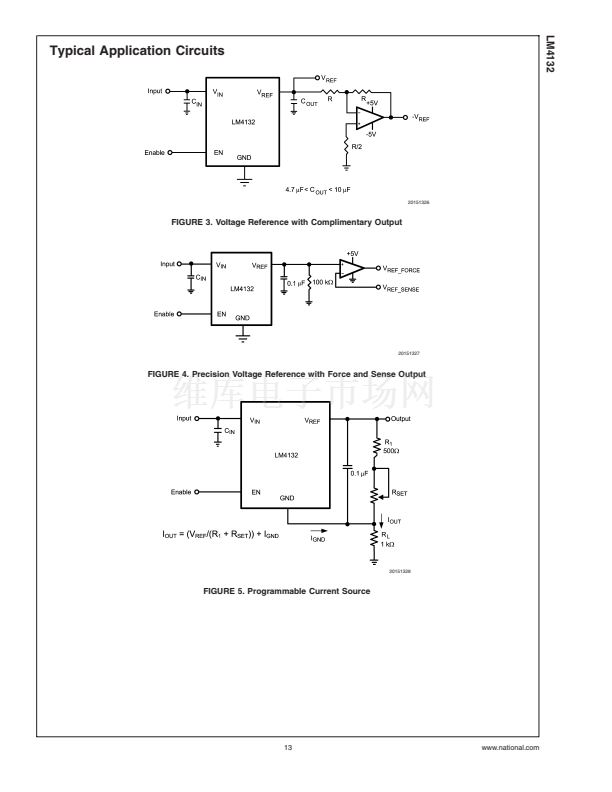
used to ensure stable operation. The value of C
sized according to the output capacitor value. The value of
鈮?/div>
C
OUT
. When no output
capacitor is used, C
IN
must have a minimum value of 0.1碌F.
Noise on the power-supply input may affect the output noise.
Larger input capacitor values (typically 4.7碌F to 22碌F) may
help reduce noise on the output and significantly reduce
overshoot during startup. Use of an additional optional by-
pass capacitor between the input and ground may help
further reduce noise on the output. With an input capacitor,
the LM4132 will drive any combination of resistance and
capacitance up to V
REF
/20mA and 10碌F respectively.
The LM4132 is designed to operate with or without an output
capacitor and is stable with capacitive loads up to 10碌F.
Connecting a capacitor between the output and ground will
significantly improve the load transient response when
switching from a light load to a heavy load. The output
capacitor should not be made arbitrarily large because it will
effect the turn-on time as well as line and load transients.
While a variety of capacitor chemistry types may be used, it
is typically advisable to use low esr ceramic capacitors. Such
capacitors provide a low impedance to high frequency sig-
nals, effectively bypassing them to ground. Bypass capaci-
tors should be mounted close to the part. Mounting bypass
capacitors close to the part will help reduce the parasitic
trace components thereby improving performance.
SHORT CIRCUITED OUTPUT
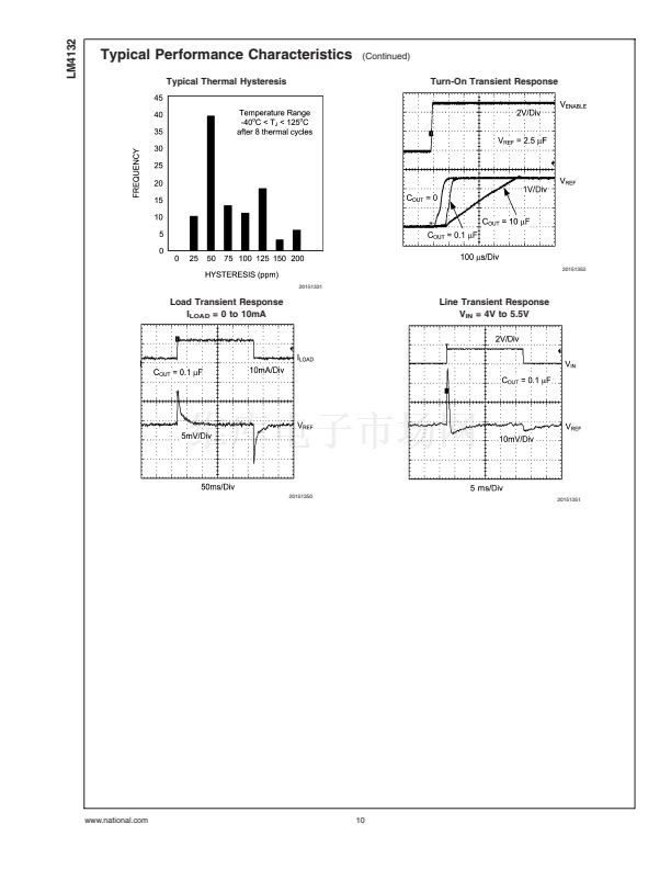
The LM4132 features indefinite short circuit protection. This
protection limits the output current to 75mA when the output
is shorted to ground.
TURN ON TIME
Turn on time is defined as the time taken for the output
voltage to rise to 90% of the preset value. The turn on time
depends on the load. The turn on time is typically 33.2碌s
when driving a 1碌F load and 78.8碌s when driving a 10碌F
load. Some users may experience an extended turn on time
(up to 10ms) under brown out conditions and low tempera-
tures (-40藲C).
11
THERMAL HYSTERESIS
Thermal hysteresis is the defined as the change in output
voltage at 25
o
C after some deviation from 25
o
C. This is to
say that thermal hysteresis is the difference in output voltage
between two points in a given temperature profile. An illus-
trative temperature profile is shown in Figure 1.
20151338
FIGURE 1. Illustrative Temperature Profile
This may be expressed analytically as the following:
Where
V
HYS
= Thermal hysteresis expressed in ppm
V
REF
= Nominal preset output voltage
V
REF1
= V
REF
before temperature fluctuation
V
REF2
= V
REF
after temperature fluctuation.
The LM4132 features a low thermal hysteresis of 75 ppm
(typical) from -40藲C to 125藲C after 8 temperature cycles.
TEMPERATURE COEFFICIENT
Temperature drift is defined as the maximum deviation in
output voltage over the operating temperature range. This
deviation over temperature may be illustrated as shown in
Figure 2.
20151339
FIGURE 2. Illustrative V
REF
vs Temperature Profile
Temperature coefficient may be expressed analytically as
the following:
www.national.com


 1
1
 2
2
 3
3
 4
4
 5
5
 6
6
 7
7
 8
8
 9
9
 10
10
 11
11
 12
12
 13
13
 14
14
 15
15
