bq24702, bq24703
SLUS553D 鈭?MAY 2003 鈭?REVISED JULY 2005
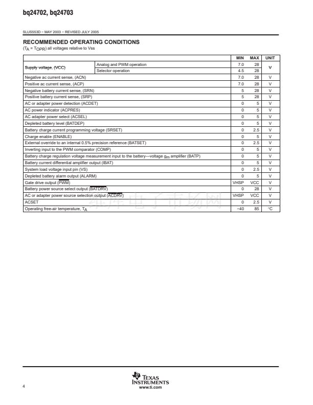
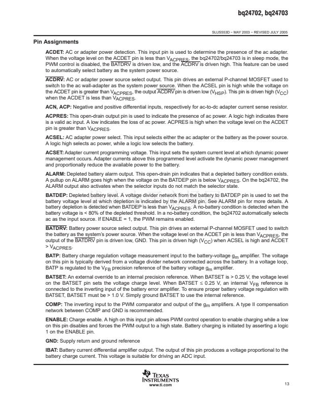
PWM:
Gate drive output pin drives the P-channel MOSFET for PWM control. The PWM control is active when
ACPRES, ACSEL, and ENABLE are high. PWM is driven low to V
HSP
and high to V
CC
.
SRN, SRP:
Differential amplifier inputs for battery current sense. These pins feed back the battery charge
current for PWM control. SRN is tied to the battery terminal. SRP is the source pin for zero volt operation.
SRSET:
Battery charge current programmed voltage. The level on this pin sets the battery charge current limit.
VCC:
Operational supply voltage.
VHSP:
The VHSP pin is connected to a 1-碌F capacitor (close to the pin) to provide a stable voltage source to
drive the gates of the external MOSFETs. VHSP = VCC 鈭?10 V for VCC > 10.5 V and VHSP = VCC 鈭?0.5 V for
VCC <10.5 V. A 13-V Zener diode should be placed between VCC and VHSP to prevent MOSFET overstress
during start-up.
VREF:
Bypassed precision voltage 5-V output. It can be used to set fixed levels on the inverting inputs of any
one of the three error amplifiers if desired. The tight tolerance is suitable for charging lithium-ion batteries.
VS:
System (Load) voltage input pin. The voltage on this pin indicates the system voltage in order to insure a
break before make transition when changing from ac power to battery power. The battery is protected from an
over-voltage condition by disabling the P-channel MOSFET connected to the BATDRV pin if the voltage at VS
is greater than BATP. This function can be eliminated by grounding the VS pin.
14
www.ti.com


 1
1
 2
2
 3
3
 4
4
 5
5
 6
6
 7
7
 8
8
 9
9
 10
10
 11
11
 12
12
 13
13
 14
14
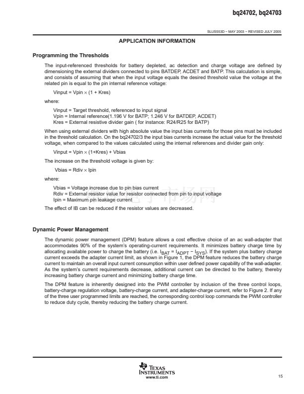 15
15
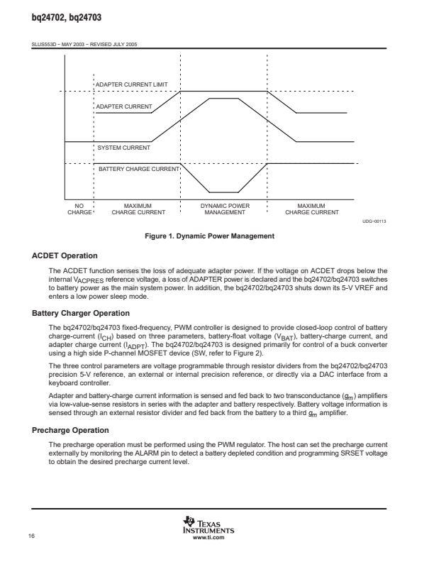 16
16
 17
17
 18
18
 19
19
 20
20
 21
21
 22
22
 23
23
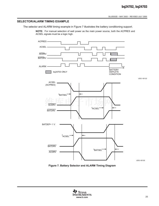
 24
24
 25
25
 26
26
 27
27
 28
28
 29
29
 30
30
 31
31
 32
32
