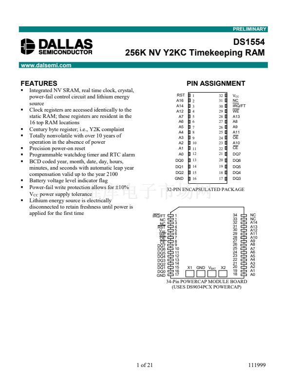
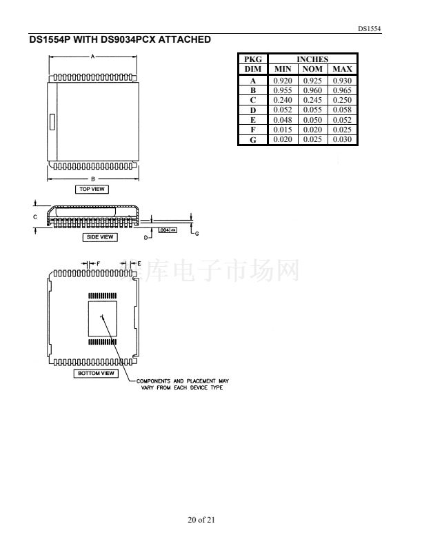
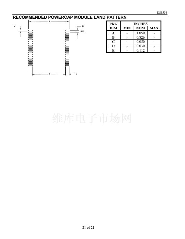
DS1554
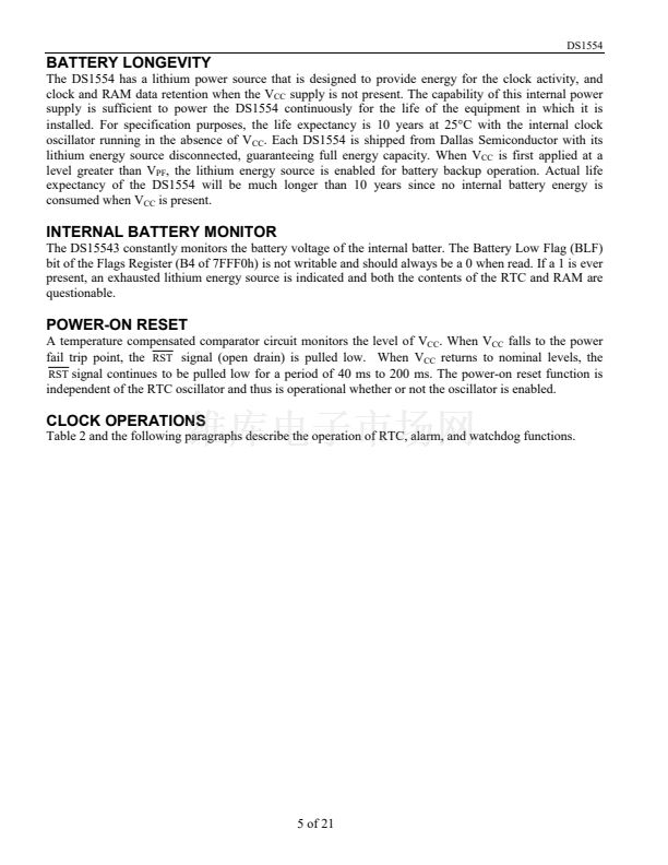
DS1554 OPERATING MODES
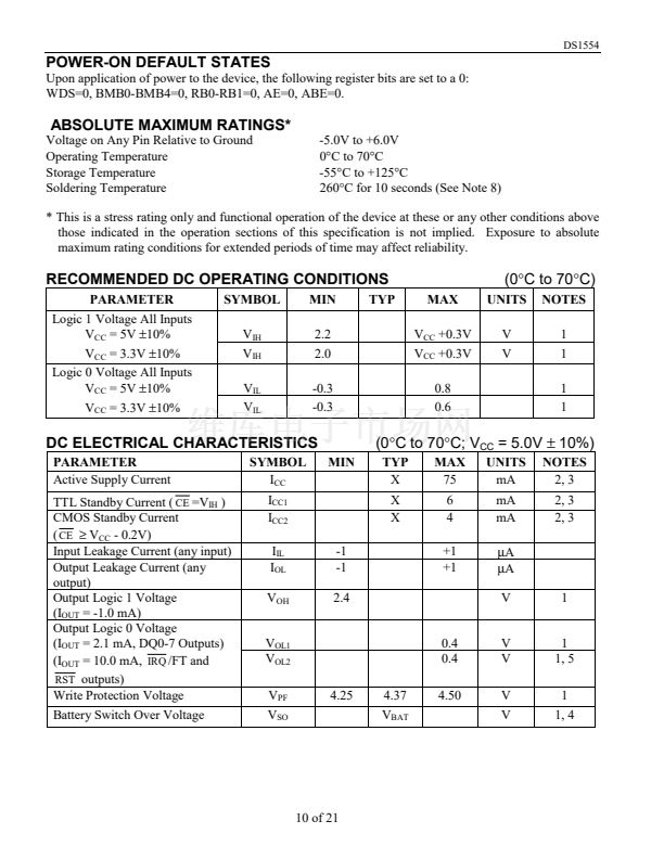
Table 1
V
CC
V
CC
> V
PF
V
SO
< V
CC
<V
PF
<V
BAT
CE
OE
WE
V
IH
V
IL
V
IL
V
IL
X
X
X
X
V
IL
V
IH
X
X
X
V
IL
V
IH
V
IH
X
X
DQ0-DQ7
HIGH-Z
D
IN
D
OUT
HIGH-Z
HIGH-Z
HIGH-Z
MODE
DESELECT
WRITE
READ
READ
DESELECT
DATA
RETENTION
POWER
STANDBY
ACTIVE
ACTIVE
ACTIVE
CMOS STANDBY
BATTERY
CURRENT
DATA READ MODE
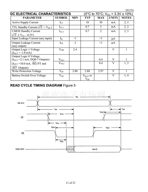
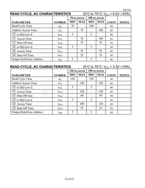
The DS1554 is in the read mode whenever
CE
(chip enable) is low and
WE
(write enable) is high. The
device architecture allows ripple-through access to any valid address location. Valid data will be available
at the DQ pins within t
AA
after the last address input is stable, providing that
CE
and
OE
access times are
satisfied. If
CE
or
OE
access times are not met, valid data will be available at the latter of chip enable
access (t
CEA
) or at output enable access time (t
OEA
). The state of the data input/output pins (DQ) is
controlled by
CE
and
OE
. If the outputs are activated before t
AA
, the data lines are driven to an
intermediate state until t
AA
. If the address inputs are changed while
CE
and
OE
remain valid, output data
will remain valid for output data hold time (t
OH
) but will then go indeterminate until the next address
access.
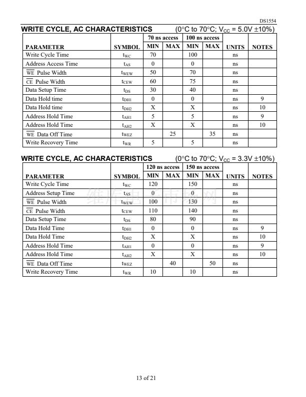
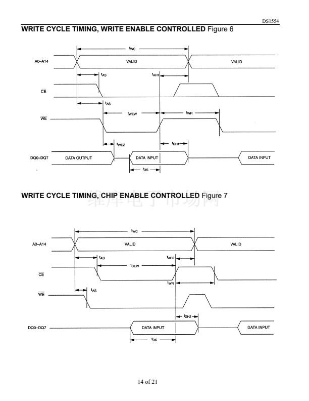
DATA WRITE MODE
The DS1554 is in the write mode whenever
WE
and
CE
are in their active state. The start of a write is
referenced to the latter occurring transition of
WE
or
CE
. The addresses must be held valid throughout
the cycle.
CE
and
WE
must return inactive for a minimum of t
WR
prior to the initiation of a subsequent
read or write cycle. Data in must be valid t
DS
prior to the end of the write and remain valid for t
DH
afterward. In a typical application, the
OE
signal will be high during a write cycle. However,
OE
can be
active provided that care is taken with the data bus to avoid bus contention. If
OE
is low prior to
WE
transitioning low, the data bus can become active with read data defined by the address inputs. A low
transition on
WE
will then disable the outputs t
WEZ
after
WE
goes active.
DATA RETENTION MODE
The 5-volt device is fully accessible and data can be written and read only when V
CC
is greater than V
PF
.
However, when V
CC
is below the power-fail point V
PF
(point at which write protection occurs) the
internal clock registers and SRAM are blocked from any access. When V
CC
falls below the battery switch
point V
SO
(battery supply level), device power is switched from the V
CC
pin to the internal backup lithium
battery. RTC operation and SRAM data are maintained from the battery until V
CC
is returned to nominal
levels.
The 3.3-volt device is fully accessible and data can be written and read only when V
CC
is greater than
V
PF
. When V
CC
falls below V
PF
, access to the device is inhibited. If V
PF
is less than V
BAT
, the device
power is switched from V
CC
to the internal backup lithium battery when V
CC
drops below V
PF
. If V
PF
is
greater than V
BAT
, the device power is switched from V
CC
to the internal backup lithium battery when
V
CC
drops below V
BAT
. RTC operation and SRAM data are maintained from the battery until V
CC
is
returned to nominal levels.
All control, data, and address signals must be powered down when V
CC
is powered down.
4 of 21


 1
1
 2
2
 3
3
 4
4
 5
5
 6
6
 7
7
 8
8
 9
9
 10
10
 11
11
 12
12
 13
13
 14
14
 15
15
 16
16
 17
17
 18
18
 19
19
 20
20
 21
21
