M24C16, M24C08, M24C04, M24C02, M24C01
SUMMARY DESCRIPTION
These I虏C-compatible electrically erasable pro-
grammable memory (EEPROM) devices are orga-
nized as 2048/1024/512/256/128 x 8 (M24C16,
M24C08, M24C04, M24C02 and M24C01).
In order to meet environmental requirements, ST
offers these devices in ECOPACK庐 packages.
ECOPACK庐 packages are Lead-free and RoHS
compliant.
ECOPACK is an ST trademark. ECOPACK speci-
fications are available at: www.st.com.
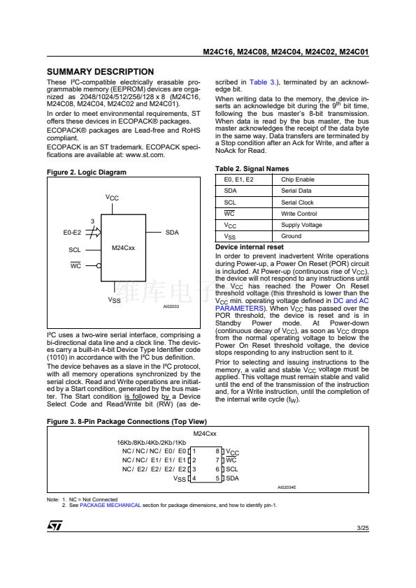
Figure 2. Logic Diagram
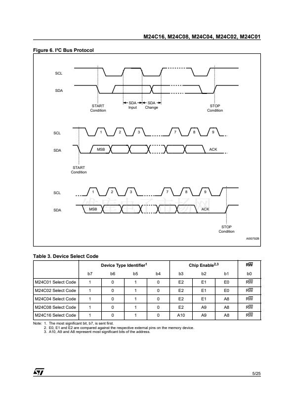
scribed in
Table 3.),
terminated by an acknowl-
edge bit.
When writing data to the memory, the device in-
serts an acknowledge bit during the 9
th
bit time,
following the bus master鈥檚 8-bit transmission.
When data is read by the bus master, the bus
master acknowledges the receipt of the data byte
in the same way. Data transfers are terminated by
a Stop condition after an Ack for Write, and after a
NoAck for Read.
Table 2. Signal Names
E0, E1, E2
SDA
Chip Enable
Serial Data
Serial Clock
Write Control
Supply Voltage
Ground
VCC
SCL
WC
3
E0-E2
SCL
WC
M24Cxx
SDA
V
CC
V
SS
VSS
AI02033
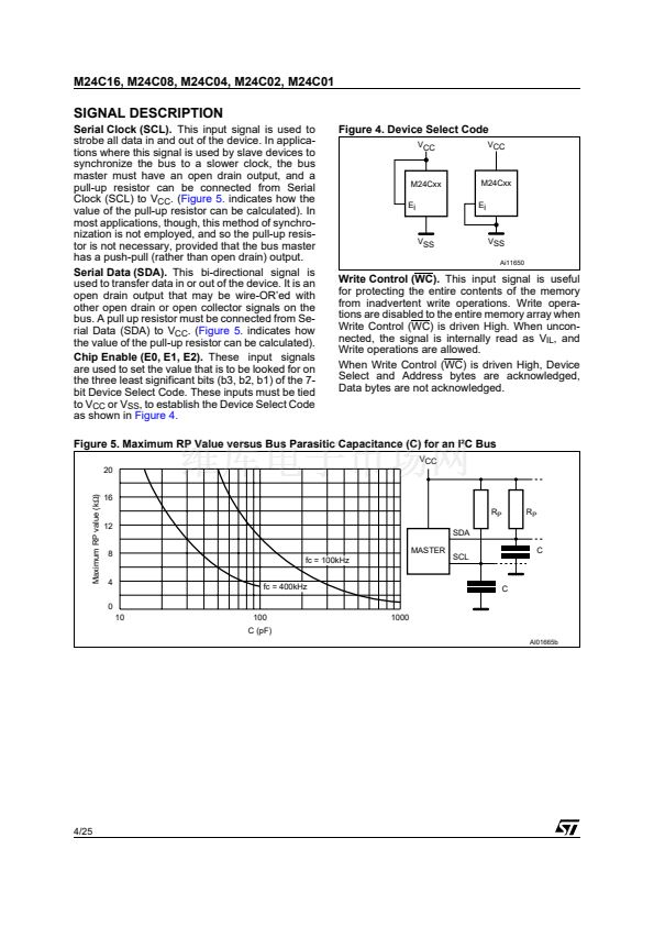
I虏C uses a two-wire serial interface, comprising a
bi-directional data line and a clock line. The devic-
es carry a built-in 4-bit Device Type Identifier code
(1010) in accordance with the I虏C bus definition.
The device behaves as a slave in the I虏C protocol,
with all memory operations synchronized by the
serial clock. Read and Write operations are initiat-
ed by a Start condition, generated by the bus mas-
ter. The Start condition is followed by a Device
Select Code and Read/Write bit (RW) (as de-
Figure 3. 8-Pin Package Connections (Top View)
Device internal reset
In order to prevent inadvertent Write operations
during Power-up, a Power On Reset (POR) circuit
is included. At Power-up (continuous rise of V
CC
),
the device will not respond to any instructions until
the V
CC
has reached the Power On Reset
threshold voltage (this threshold is lower than the
V
CC
min. operating voltage defined in
DC and AC
PARAMETERS).
When V
CC
has passed over the
POR threshold, the device is reset and is in
Standby
Power
mode.
At
Power-down
(continuous decay of V
CC
), as soon as V
CC
drops
from the normal operating voltage to below the
Power On Reset threshold voltage, the device
stops responding to any instruction sent to it.
Prior to selecting and issuing instructions to the
memory, a valid and stable V
CC
voltage must be
applied. This voltage must remain stable and valid
until the end of the transmission of the instruction
and, for a Write instruction, until the completion of
the internal write cycle (t
W
).
M24Cxx
16Kb /8Kb /4Kb /2Kb /1Kb
NC / NC / NC / E0 / E0
NC / NC / E1 / E1 / E1
NC / E2 / E2 / E2 / E2
VSS
1
2
3
4
8
7
6
5
VCC
WC
SCL
SDA
AI02034E
Note: 1. NC = Not Connected
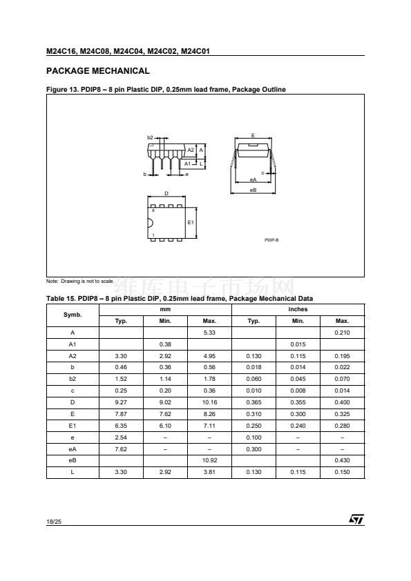
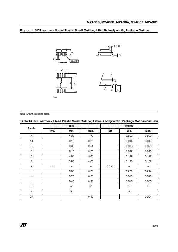
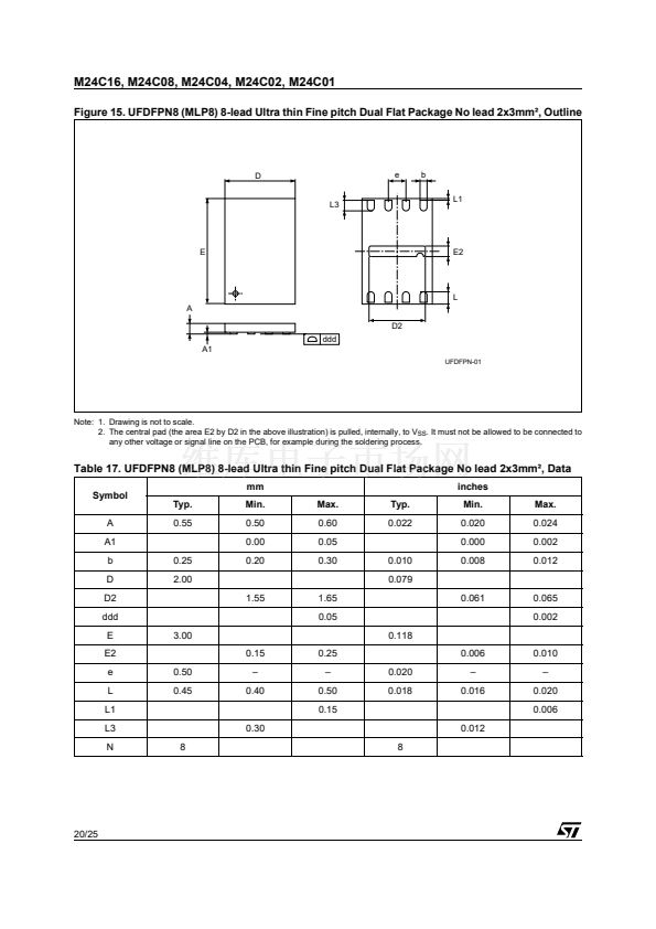
2. See
PACKAGE MECHANICAL
section for package dimensions, and how to identify pin-1.
3/25


 1
1
 2
2
 3
3
 4
4
 5
5
 6
6
 7
7
 8
8
 9
9
 10
10
 11
11
 12
12
 13
13
 14
14
 15
15
 16
16
 17
17
 18
18
 19
19
 20
20
 21
21
 22
22
 23
23
 24
24
 25
25
