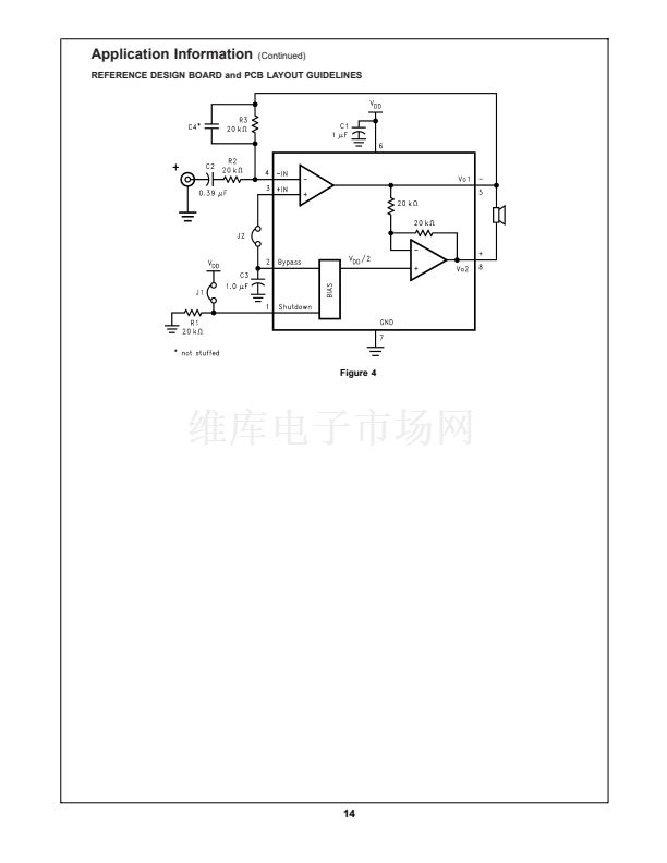
Application Information
(Continued)
Mono
HWD2119
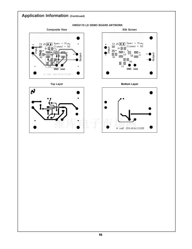
Reference Design Boards
Bill of Material for all Demo Boards
Item
1
10
20
21
25
30
35
Part Number
482911183-001
151911207-001
151911207-002
152911207-001
472911207-001
210007039-002
Part Description
HWD2119
Audio AMP
Tant Cap 1uF 16V 10
Cer Cap 0.39uF 50V Z5U 20% 1210
Tant Cap 1uF 16V 10
Res 20K Ohm 1/10W 5
Jumper Header Vertical Mount 2X1
0.100
1
1
1
3
2
Qty
1
1
U1
C1
C2
C3
R1, R2, R3
J1, J2
Ref Designator
551011208-001
HWD2119
Mono Reference Design Board
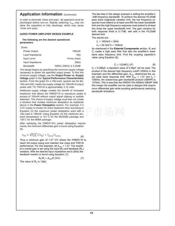
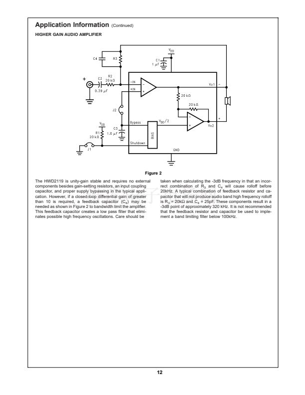
PCB LAYOUT GUIDELINES
This section provides practical guidelines for mixed signal
PCB layout that involves various digital/analog power and
ground traces. Designers should note that these are only
鈥檙ule-of-thumb鈥?recommendations and the actual results will
depend heavily on the final layout.
General Mixed Signal Layout Recommendation
Power and Ground Circuits
For two layer mixed signal design, it is important to isolate
the digital power and ground trace paths from the analog
power and ground trace paths. Star trace routing techniques
(bringing individual traces back to a central point rather than
daisy chaining traces together in a serial manner) can have
a major impact on low level signal performance. Star trace
routing refers to using individual traces to feed power and
ground to each circuit or even device. This technique will
take require a greater amount of design time but will not
increase the final price of the board. The only extra parts
required will be some jumpers.
Single-Point Power / Ground Connections
The analog power traces should be connected to the digital
traces through a single point (link). A 鈥橮i-filter鈥?can be helpful
in minimizing high frequency noise coupling between the
analog and digital sections. It is further recommended to put
digital and analog power traces over the corresponding digi-
tal and analog ground traces to minimize noise coupling.
Placement of Digital and Analog Components
All digital components and high-speed digital signals traces
should be located as far away as possible from analog
components and circuit traces.
Avoiding Typical Design / Layout Problems
Avoid ground loops or running digital and analog traces
parallel to each other (side-by-side) on the same PCB layer.
When traces must cross over each other do it at 90 degrees.
Running digital and analog traces at 90 degrees to each
other from the top to the bottom side as much as possible will
minimize capacitive noise coupling and cross talk.
17


 1
1
 2
2
 3
3
 4
4
 5
5
 6
6
 7
7
 8
8
 9
9
 10
10
 11
11
 12
12
 13
13
 14
14
 15
15
 16
16
 17
17
 18
18
 19
19
 20
20
 21
21
