Electrical Characteristics V
DD
= 3V
The following specifications apply for V
DD
25藲C. (Continued)
(Notes 2, 3)
= 3V and R
L
= 16鈩?load unless otherwise stated. Limits apply to T
A
=
Note 1:
See AN-450 鈥橲urface Mounting and their Effects on Product Reliability鈥?for other methods of soldering surface mount devices.
Note 2:
All voltages are measured with respect to the ground pin, unless otherwise specified.
Note 3:
Absolute Maximum Ratings
indicate limits beyond which damage to the device may occur.
Operating Ratings
indicate conditions for which the device is
functional, but do not guarantee specific performance limits.
Electrical Characteristics
state DC and AC electrical specifications under particular test conditions which
guarantee specific performance limits. This assumes that the device is within the Operating Ratings. Specifications are not guaranteed for parameters where no limit
is given. However, the typical value is a good indication of device鈥檚 performance.
Note 4:
The maximum power dissipation must be derated at elevated temperatures and is dictated by T
JMAX
,
胃
JA
, and the ambient temperature T
A
. The maximum
allowable power dissipation is P
DMAX
= (T
JMAX
鈥揟
A
)/胃
JA
. For the
HWD2119,
T
JMAX
= 150藲C and the typical junction-to-ambient thermal resistance (胃
JA
) when board
mounted is 210藲C/W for the MSOP package and 170藲C/W for the SOP package.
Note 5:
Human body model, 100pF discharged through a 1.5 k鈩?resistor.
Note 6:
Machine Model, 220pF鈥?40pF capacitor is discharged through all pins.
Note 7:
Typical specifications are specified at 25藲C and represent the parametric norm.
Note 8:
Tested limits are guaranteed to National鈥檚 AOQL (Average Outgoing Quality Level).
Note 9:
Datasheet min/max specification limits are guaranteed by designs, test, or statistical analysis.
Note 10:
The given
胃
JA
is for an
HWD2119
package in an LDA08B with the Exposed-DAP soldered to a printed circuit board copper pad with an area equivalent to
that of the Exposed-DAP itself. The Exposed-DAP of the LDA08B package should be electrically connected to GND or an electrically isolated copper area.
Note 11:
The given
胃
JA
is for an
HWD2119
package in an LDA08B with the Exposed-DAP not soldered to any printed circuit board copper.
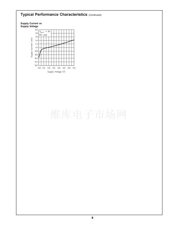
Note 12:
The shutdown pin (pin1) should be driven as close as possible to V
DD
for minimum current in Shutdown Mode.
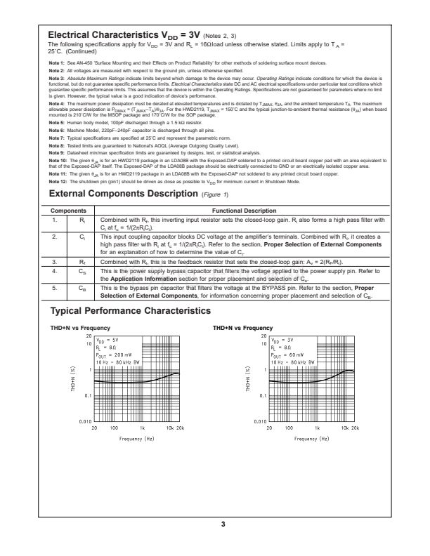
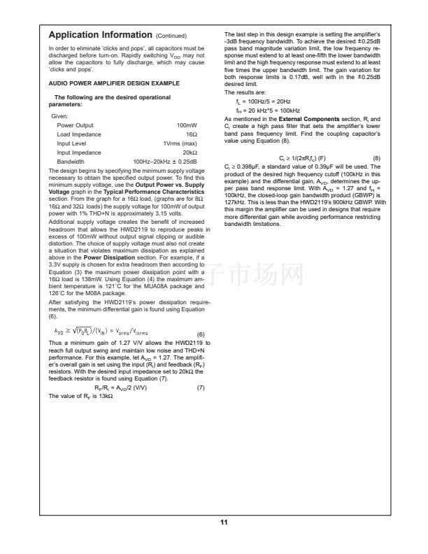
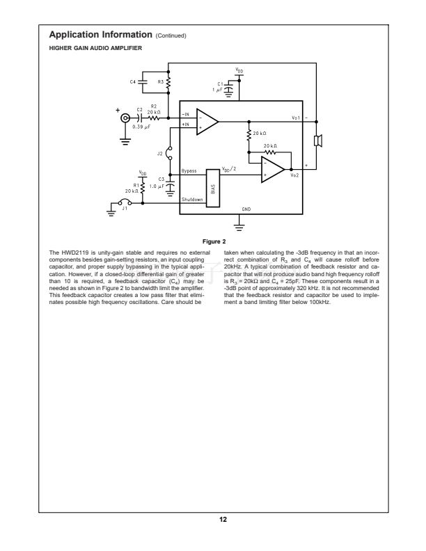
External Components Description
Components
1.
2.
R
i
C
i
(Figure
1)
Functional Description
Combined with R
f
, this inverting input resistor sets the closed-loop gain. R
i
also forms a high pass filter with
C
i
at f
c
= 1/(2蟺R
i
C
i
).
This input coupling capacitor blocks DC voltage at the amplifier鈥檚 terminals. Combined with R
i
, it creates a
high pass filter with R
i
at f
c
= 1/(2蟺R
i
C
i
). Refer to the section,
Proper Selection of External Components
for an explanation of how to determine the value of C
i
.
Combined with R
i
, this is the feedback resistor that sets the closed-loop gain: A
v
= 2(R
F
/R
i
).
This is the power supply bypass capacitor that filters the voltage applied to the power supply pin. Refer to
the
Application Information
section for proper placement and selection of C
s
.
This is the bypass pin capacitor that filters the voltage at the BYPASS pin. Refer to the section,
Proper
Selection of External Components,
for information concerning proper placement and selection of C
B
.
3.
4.
5.
R
f
C
S
C
B
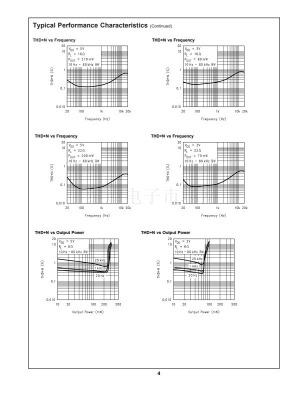
Typical Performance Characteristics
THD+N vs Frequency
THD+N vs Frequency
3


 1
1
 2
2
 3
3
 4
4
 5
5
 6
6
 7
7
 8
8
 9
9
 10
10
 11
11
 12
12
 13
13
 14
14
 15
15
 16
16
 17
17
 18
18
 19
19
 20
20
 21
21
