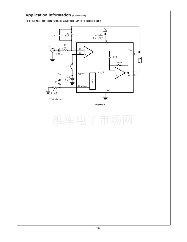
Application Information
BRIDGE CONFIGURATION EXPLANATION
As shown in
Figure 1,
the
HWD2119
consist of two operational
amplifiers. External resistors, R
i
and R
F
set the closed-loop
gain of the first amplifier (and the amplifier overall), whereas
two internal 20k鈩?resistors set the second amplifier鈥檚 gain at
-1. The
HWD2119
is typically used to drive a speaker con-
nected between the two amplifier outputs.
Figure 1
shows that the output of Amp1 servers as the input
to Amp2, which results in both amplifiers producing signals
identical in magnitude but 180藲 out of phase. Taking advan-
tage of this phase difference, a load is placed between V
01
and V
02
and driven differentially (commonly referred to as
鈥檅ridge mode鈥?. This results in a differential gain of
A
VD
= 2 *(R
f
/R
i
)
(1)
Bridge mode is different from single-ended amplifiers that
drive loads connected between a single amplifier鈥檚 output
and ground. For a given supply voltage, bridge mode has a
distinct advantage over the single-ended configuration: its
differential output doubles the voltage swing across the load.
This results in four times the output power when compared
to a single-ended amplifier under the same conditions. This
increase in attainable output assumes that the amplifier is
not current limited or the output signal is not clipped. To
ensure minimum output signal clipping when choosing an
amplifier鈥檚 closed-loop gain, refer to the
Audio Power Am-
plifier Design Example
section.
Another advantage of the differential bridge output is no net
DC voltage across the load. This results from biasing V
01
and V
02
at half-supply. This eliminates the coupling capacitor
that single supply, single-ended amplifiers require. Eliminat-
ing an output coupling capacitor in a single-ended configu-
ration forces a single supply amplifier鈥檚 half-supply bias volt-
age across the load. The current flow created by the half-
supply bias voltage increases internal IC power dissipation
and may permanently damage loads such as speakers.
POWER DISSIPATION
Power dissipation is a major concern when designing a
successful bridged or single-ended amplifier. Equation (2)
states the maximum power dissipation point for a single-
ended amplifier operating at a given supply voltage and
driving a specified load.
P
DMAX
= (V
DD
)
2
/(2蟺
2
R
L
) (W) Single-ended
(2)
However, a direct consequence of the increased power de-
livered to the load by a bridged amplifier is an increase in the
internal power dissipation point for a bridge amplifier oper-
ating at the same given conditions. Equation (3) states the
maximum power dissipation point for a bridged amplifier
operating at a given supply voltage and driving a specified
load.
P
DMAX
= 4(V
DD
)
2
/(2蟺
2
R
L
) (W) Bridge Mode
(3)
The
HWD2119
has two operational amplifiers in one package
and the maximum internal power dissipation is four times
that of a single-ended amplifier. However, even with this
substantial increase in power dissipation, the
HWD2119
does
not require heatsinking. From Equation (3), assuming a 5V
power supply and an 8鈩?load, the maximum power dissipa-
tion point is 633mW. The maximum power dissipation point
obtained from Equation (3) must not exceed the power dis-
sipation predicted by Equation (4):
P
DMAX
= (T
JMAX
- T
A
)/胃
JA
(W)
(4)
For the micro MUA08A package,
胃
JA
= 210藲C/W, for the
M08A package,
胃
JA
= 170藲C/W , and T
JMAX
= 150藲C for the
HWD2119.
For a given ambient temperature,
A
T Equation (4)
,
can be used to find the maximum internal power dissipation
supported by the IC packaging. If the result of Equation (3) is
greater than the result of Equation (4), then decrease the
supply voltage, increase the load impedance, or reduce the
ambient temperature. For a typical application using the
M08A packaged
HWD2119
with a 5V power supply and an 8鈩?/div>
load, the maximum ambient temperature that does not vio-
late the maximum junction temperature is approximately
42藲C. If a MUA08A packaged part is used instead with the
same supply voltage and load, the maximum ambient tem-
perature is 17藲C. In both cases, it is assumed that a device
is a surface mount part operating around the maximum
power dissipation point. The assumption that the device is
operating around the maximum power dissipation point is
incorrect for an 8鈩?load. The maximum power dissipation
point occurs when the output power is equal to the maximum
power dissipation or 50% efficiency. The
HWD2119
is not
capable of the output power level (633mW) required to op-
erate at the maximum power dissipation point for an 8鈩?load.
To find the maximum power dissipation, the graph
Power
Dissipation vs. Output Power
must be used. From the
graph, the maximum power dissipation for an 8鈩?load and a
5V supply is approximately 575mW. Substituting this value
back into equation (4) for P
DMAX
and using
胃
JA
= 210藲C/W
for the MUA08A package, the maximum ambient tempera-
ture is calculated to be 29藲C. Using
胃
JA
= 170藲C/W for the
M08A package, the maximum ambient temperature is 52藲C.
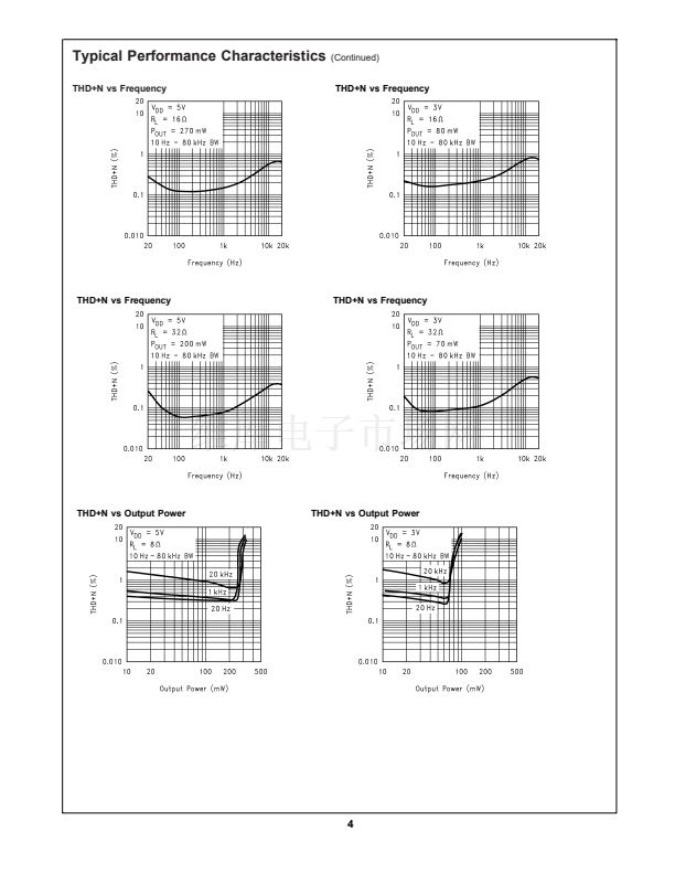
Refer to the
Typical Performance Characteristics
curves
for power dissipation information for lower output powers
and maximum power dissipation for each package at a given
ambient temperature.
POWER SUPPLY BYPASSING
As with any power amplifier, proper supply bypassing is
critical for low noise performance and high power supply
rejection. The capacitors connected to the bypass and power
supply pins should be placed as close to the
HWD2119
as
possible. The capacitor connected between the bypass pin
and ground improves the internal bias voltage鈥檚 stability,
producing improved PSRR. The improvements to PSRR
increase as the bypass pin capacitor value increases. Typi-
cal applications employ a 5V regulator with 10碌F and 0.1碌F
filter capacitors that aid in supply stability. Their presence,
however, does not eliminate the need for bypassing the
supply nodes of the
HWD2119.
The selection of bypass ca-
pacitor values, especially C
B
, depends on desired PSRR
requirements, click and pop performance as explained in the
section,
Proper Selection of External Components,
as
well as system cost and size constraints.
SHUTDOWN FUNCTION
The voltage applied to the
HWD2119鈥檚
SHUTDOWN pin con-
trols the shutdown function. Activate micro-power shutdown
by applying V
DD
to the SHUTDOWN pin. When active, the
HWD2119鈥檚
micro-power shutdown feature turns off the ampli-
fier鈥檚 bias circuitry, reducing the supply current. The logic
threshold is typically 1/2V
DD
. The low 0.7碌A typical shut-
down current is achieved by applying a voltage that is as
near as V
DD
as possible to the SHUTDOWN pin. A voltage
that is less than V
DD
may increase the shutdown current.
Avoid intermittent or unexpected micro-power shutdown by
ensuring that the SHUTDOWN pin is not left floating but
connected to either V
DD
or GND.
9


 1
1
 2
2
 3
3
 4
4
 5
5
 6
6
 7
7
 8
8
 9
9
 10
10
 11
11
 12
12
 13
13
 14
14
 15
15
 16
16
 17
17
 18
18
 19
19
 20
20
 21
21
