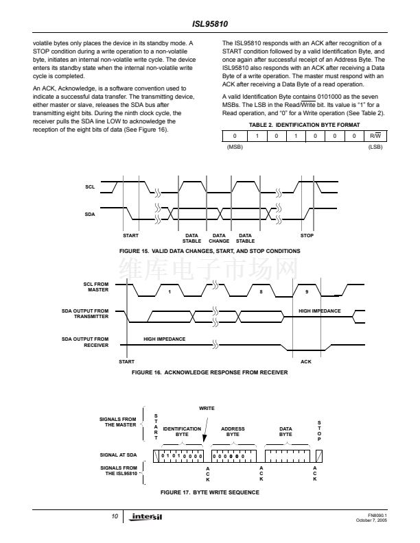
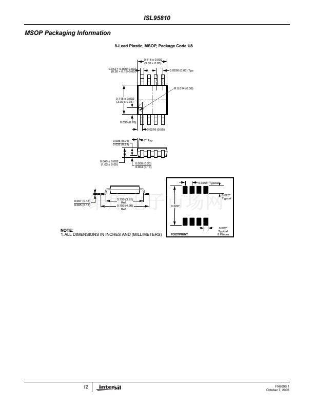
ISL95810
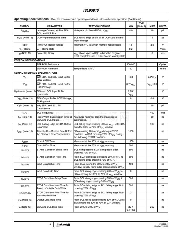
Operating Specifications
Over the recommended operating conditions unless otherwise specified.
(Continued)
SYMBOL
I
LkgDig
t
DCP
(Note 13)
Vpor
V
CC
Ramp
t
D
(Note 13)
PARAMETER
Leakage Current, at Pins SDA,
SCL, and WP Pins
DCP Wiper Response Time
Power-On Recall Voltage
V
CC
Ramp Rate
Power-Up Delay
V
CC
above Vpor, to DCP Initial Value Register
recall completed, and I
2
C Interface in standby state
200,000
Temperature
鈮?5掳C
50
-0.3
0.7*V
CC
0.05*
V
CC
0
0.4
10
400
50
900
1300
0.3*V
CC
V
CC
+0.3
TEST CONDITIONS
Voltage at pin from GND to V
CC
SCL falling edge of last bit of DCP Data Byte to
wiper change
Minimum V
CC
at which memory recall occurs
1.8
0.2
3
MIN
-10
TYP
(Note 1)
MAX
10
1
2.6
UNITS
碌A
碌s
V
V/ms
ms
EEPROM SPECIFICATIONS
EEPROM Endurance
EEPROM Retention
SERIAL INTERFACE SPECIFICATIONS
V
IL
V
IH
WP, SDA, and SCL Input Buffer
LOW Voltage
WP, SDA, and SCL Input Buffer
HIGH Voltage
V
V
V
V
pF
kHz
ns
ns
ns
Cycles
Years
Hysteresis (Note 13) SDA and SCL Input Buffer
Hysteresis
V
OL
(Note 13)
Cpin (Note 13)
f
SCL
t
IN
(Note 13)
t
AA
(Note 13)
t
BUF
(Note 13)
SDA Output Buffer LOW Voltage,
Sinking 4mA
WP, SDA, and SCL Pin
Capacitance
SCL Frequency
Pulse Width Suppression Time at Any pulse narrower than the max spec is
SDA and SCL Inputs
suppressed.
SCL Falling Edge to SDA Output
Data Valid
SCL falling edge crossing 30% of V
CC
, until SDA
exits the 30% to 70% of V
CC
window.
Time the Bus Must be Free Before SDA crossing 70% of V
CC
during a STOP
the Start of a New Transmission condition, to SDA crossing 70% of V
CC
during
the following START condition.
Clock LOW Time
Clock HIGH Time
START Condition Setup Time
START Condition Hold Time
Input Data Setup Time
Input Data Hold Time
STOP Condition Setup Time
STOP Condition Hold Time for
Read, or Volatile Only Write
STOP Condition Hold Time for
Non-Volatile Write
Output Data Hold Time
SDA and SCL Rise Time
Measured at the 30% of V
CC
crossing.
Measured at the 70% of V
CC
crossing.
SCL rising edge to SDA falling edge. Both
crossing 70% of V
CC
.
From SDA falling edge crossing 30% of V
CC
to
SCL falling edge crossing 70% of V
CC
.
From SDA exiting the 30% to 70% of V
CC
window, to SCL rising edge crossing 30% of V
CC
From SCL rising edge crossing 70% of V
CC
to
SDA entering the 30% to 70% of V
CC
window.
From SCL rising edge crossing 70% of V
CC
, to
SDA rising edge crossing 30% of V
CC
.
From SDA rising edge to SCL falling edge. Both
crossing 70% of V
CC
.
From SDA rising edge to SCL falling edge. Both
crossing 70% of V
CC
.
From SCL falling edge crossing 30% of V
CC
, until
SDA enters the 30% to 70% of V
CC
window.
From 30% to 70% of V
CC
t
LOW
t
HIGH
t
SU:STA
t
HD:STA
t
SU:DAT
t
HD:DAT
t
SU:STO
t
HD:STO
t
HD:STO:NV
t
DH
(Note 13)
t
R
(Note 13)
1300
600
600
600
100
0
600
600
2
0
20 +
0.1 * Cb
250
ns
ns
ns
ns
ns
ns
ns
ns
碌s
ns
ns
4
FN8090.1
October 7, 2005


 1
1
 2
2
 3
3
 4
4
 5
5
 6
6
 7
7
 8
8
 9
9
 10
10
 11
11
 12
12
 13
13
