ISL95810
Principles of Operation
The ISL95810 is an integrated circuit incorporating one DCP
with its associated registers, non-volatile memory, and a I
2
C
serial interface providing direct communication between a
host and the potentiometer and memory.
鈥?A write operation to addresses 0 writes the same value to
the WR and IVR of the corresponding DCP.
When the byte at address 2 is 80h (128 decimal):
鈥?A read operation to addresses 0 outputs the value of the
volatile WR.
鈥?A write operation to addresses 0 only writes to the
corresponding volatile WR.
It is not possible to write to an IVR without writing the same
value to its corresponding WR.
00h and 80h are the only values that should be written to
address 2. All other values are reserved and must not be
written to address 2.
The ISL95810 is pre-programed with 80h in the IVR.
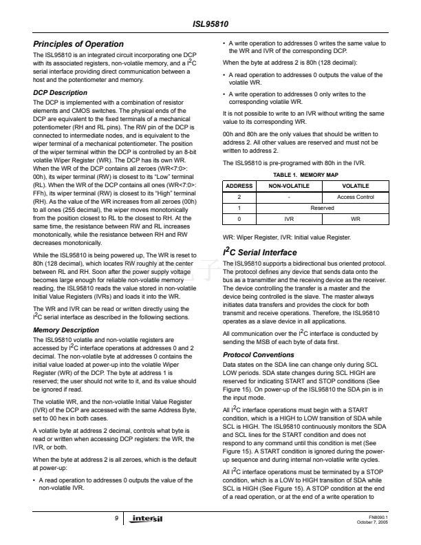
TABLE 1. MEMORY MAP
ADDRESS
2
1
0
IVR
NON-VOLATILE
-
Reserved
WR
VOLATILE
Access Control
DCP Description
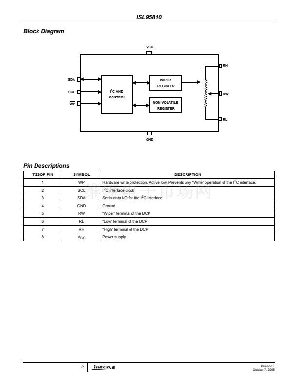
The DCP is implemented with a combination of resistor
elements and CMOS switches. The physical ends of the
DCP are equivalent to the fixed terminals of a mechanical
potentiometer (RH and RL pins). The RW pin of the DCP is
connected to intermediate nodes, and is equivalent to the
wiper terminal of a mechanical potentiometer. The position
of the wiper terminal within the DCP is controlled by an 8-bit
volatile Wiper Register (WR). The DCP has its own WR.
When the WR of the DCP contains all zeroes (WR<7:0>:
00h), its wiper terminal (RW) is closest to its 鈥淟ow鈥?terminal
(RL). When the WR of the DCP contains all ones (WR<7:0>:
FFh), its wiper terminal (RW) is closest to its 鈥淗igh鈥?terminal
(RH). As the value of the WR increases from all zeroes (00h)
to all ones (255 decimal), the wiper moves monotonically
from the position closest to RL to the closest to RH. At the
same time, the resistance between RW and RL increases
monotonically, while the resistance between RH and RW
decreases monotonically.
While the ISL95810 is being powered up, The WR is reset to
80h (128 decimal), which locates RW roughly at the center
between RL and RH. Soon after the power supply voltage
becomes large enough for reliable non-volatile memory
reading, the ISL95810 reads the value stored in non-volatile
Initial Value Registers (IVRs) and loads it into the WR.
The WR and IVR can be read or written directly using the
I
2
C serial interface as described in the following sections.
WR: Wiper Register, IVR: Initial value Register.
I
2
C Serial Interface
The ISL95810 supports a bidirectional bus oriented protocol.
The protocol defines any device that sends data onto the
bus as a transmitter and the receiving device as the receiver.
The device controlling the transfer is a master and the
device being controlled is the slave. The master always
initiates data transfers and provides the clock for both
transmit and receive operations. Therefore, the ISL95810
operates as a slave device in all applications.
All communication over the I
2
C interface is conducted by
sending the MSB of each byte of data first.
Memory Description
The ISL95810 volatile and non-volatile registers are
accessed by I
2
C interface operations at addresses 0 and 2
decimal. The non-volatile byte at addresses 0 contains the
initial value loaded at power-up into the volatile Wiper
Register (WR) of the DCP. The byte at address 1 is
reserved; the user should not write to it, and its value should
be ignored if read.
The volatile WR, and the non-volatile Initial Value Register
(IVR) of the DCP are accessed with the same Address Byte,
set to 00 hex in both cases.
A volatile byte at address 2 decimal, controls what byte is
read or written when accessing DCP registers: the WR, the
IVR, or both.
When the byte at address 2 is all zeroes, which is the default
at power-up:
鈥?A read operation to addresses 0 outputs the value of the
non-volatile IVR.
Protocol Conventions
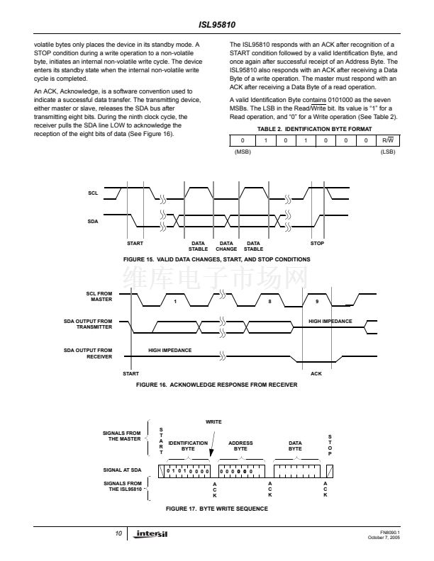
Data states on the SDA line can change only during SCL
LOW periods. SDA state changes during SCL HIGH are
reserved for indicating START and STOP conditions (See
Figure 15). On power-up of the ISL95810 the SDA pin is in
the input mode.
All I
2
C interface operations must begin with a START
condition, which is a HIGH to LOW transition of SDA while
SCL is HIGH. The ISL95810 continuously monitors the SDA
and SCL lines for the START condition and does not
respond to any command until this condition is met (See
Figure 15). A START condition is ignored during the power-
up sequence and during internal non-volatile write cycles.
All I
2
C interface operations must be terminated by a STOP
condition, which is a LOW to HIGH transition of SDA while
SCL is HIGH (See Figure 15). A STOP condition at the end
of a read operation, or at the end of a write operation to
FN8090.1
October 7, 2005
9


 1
1
 2
2
 3
3
 4
4
 5
5
 6
6
 7
7
 8
8
 9
9
 10
10
 11
11
 12
12
 13
13
