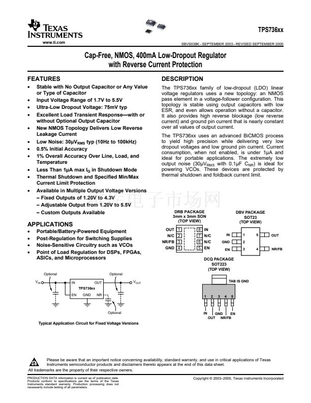
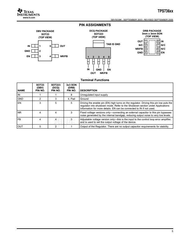
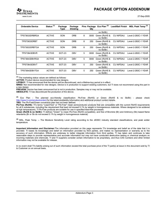
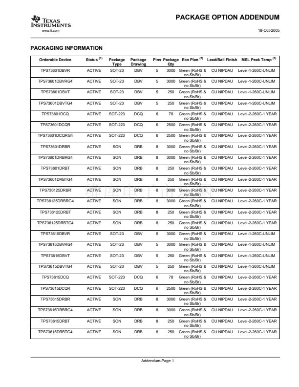
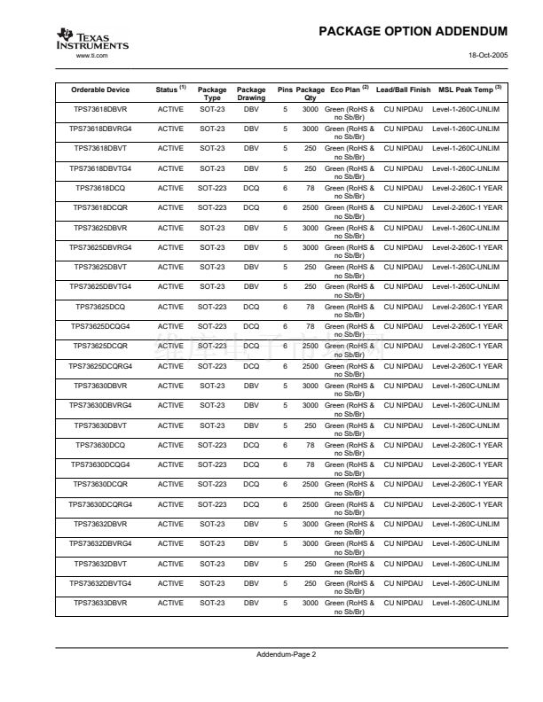
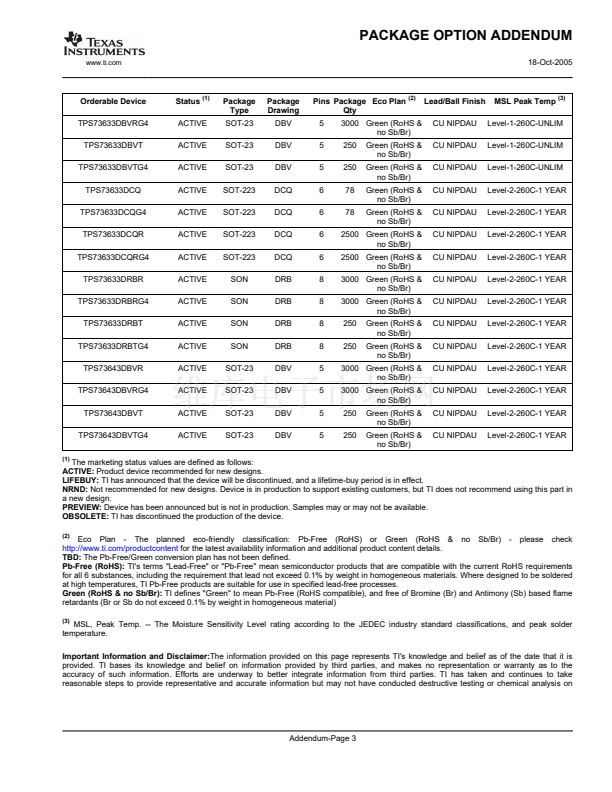
TPS736xx
www.ti.com
SBVS038K 鈥?SEPTEMBER 2003 鈥?REVISED SEPTEMBER 2005
APPLICATION INFORMATION
The TPS736xx belongs to a family of new generation
LDO regulators that use an NMOS pass transistor to
achieve ultra-low-dropout performance, reverse cur-
rent blockage, and freedom from output capacitor
constraints. These features, combined with low noise
and an enable input, make the TPS736xx ideal for
portable applications. This regulator family offers a
wide selection of fixed output voltage versions and an
adjustable output version. All versions have thermal
and over-current protection, including foldback cur-
rent limit.
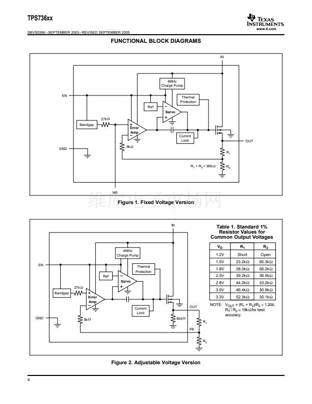
Figure 31
shows the basic circuit connections for the
fixed voltage models.
Figure 32
gives the connections
for the adjustable output version (TPS73601). R
1
and
R
2
can be calculated for any output voltage using the
formula in
Figure 32.
Sample resistor values for
common output voltages are shown in
Figure 2.
For
best accuracy, make the parallel combination of R
1
and R
2
approximately 19k鈩?
Optional input capacitor.
May improve source
impedance, noise, or PSRR.
V
IN
IN
EN
GND
Optional output capacitor.
May improve load transient,
noise, or PSRR.
OUT
TPS736xx
NR
V
OUT
Input and Output Capacitor Requirements
Although an input capacitor is not required for stab-
ility, it is good analog design practice to connect a
0.1碌F to 1碌F low ESR capacitor across the input
supply near the regulator. This will counteract reac-
tive input sources and improves transient response,
noise rejection, and ripple rejection. A higher-value
capacitor may be necessary if large, fast rise-time
load transients are anticipated or the device is lo-
cated several inches from the power source.
The TPS736xx does not require an output capacitor
for stability and has maximum phase margin with no
capacitor. It is designed to be stable for all available
types and values of capacitors. In applications where
V
IN
鈥?V
OUT
< 0.5V and multiple low ESR capacitors
are in parallel, ringing may occur when the product of
C
OUT
and total ESR drops below 50n鈩. Total ESR
includes all parasitic resistances, including capacitor
ESR and board, socket, and solder joint resistance.
In most applications, the sum of capacitor ESR and
trace resistance will meet this requirement.
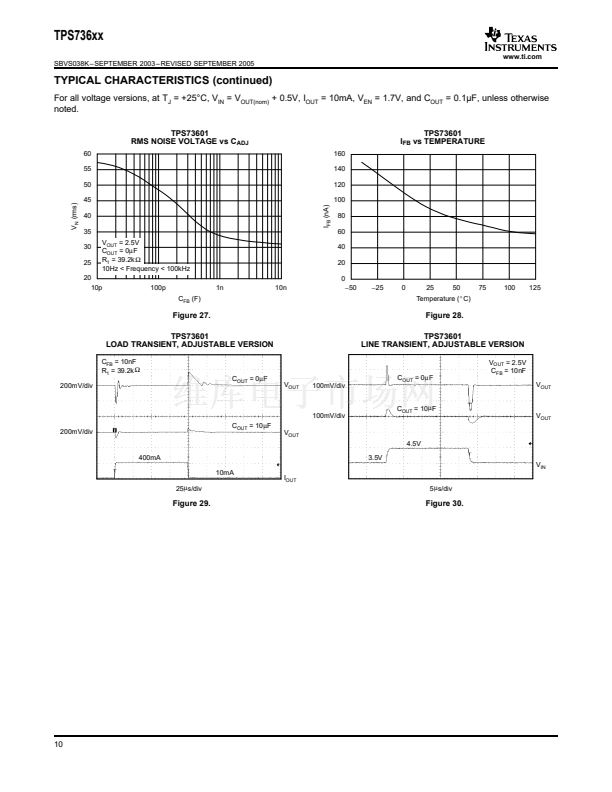
Output Noise
A precision band-gap reference is used to generate
the internal reference voltage, V
REF
. This reference is
the dominant noise source within the TPS736xx and
it generates approximately 32碌V
RMS
(10Hz to
100kHz) at the reference output (NR). The regulator
control loop gains up the reference noise with the
same gain as the reference voltage, so that the noise
voltage of the regulator is approximately given by:
V
N
+
32mV
RMS
(R
1
)
R
2
)
+
32mV
RMS
R
2
V
OUT
V
REF
Optional bypass
capacitor to reduce
output noise.
Figure 31. Typical Application Circuit for
Fixed-Voltage Versions
(1)
Optional input capacitor.
May improve source
impedance, noise, or PSRR.
V
IN
IN
OUT
TPS736xx
GND
FB
Optional output capacitor.
May improve load transient,
noise, or PSRR.
V
OUT
R
1
C
FB
Since the value of V
REF
is 1.2V, this relationship
reduces to:
mV
RMS
V
N
(mV
RMS
)
+
27
V
OUT
(V)
V
(2)
for the case of no C
NR
.
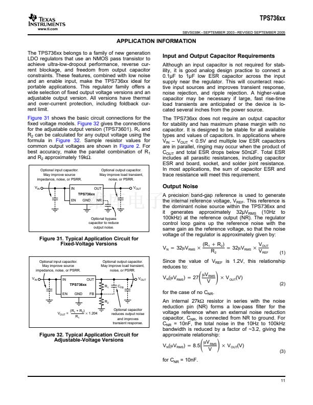
An internal 27k鈩?resistor in series with the noise
reduction pin (NR) forms a low-pass filter for the
voltage reference when an external noise reduction
capacitor, C
NR
, is connected from NR to ground. For
C
NR
= 10nF, the total noise in the 10Hz to 100kHz
bandwidth is reduced by a factor of ~3.2, giving the
approximate relationship:
mV
RMS
V
N
(mV
RMS
) + 8.5
V
OUT
(V)
V
(3)
for C
NR
= 10nF.
EN
R
2
V
OUT
=
(R
1
+ R
2
)
R
1
脳
1.204
Optional capacitor
reduces output noise
and improves
transient response.
Figure 32. Typical Application Circuit for
Adjustable-Voltage Versions
11


 1
1
 2
2
 3
3
 4
4
 5
5
 6
6
 7
7
 8
8
 9
9
 10
10
 11
11
 12
12
 13
13
 14
14
 15
15
 16
16
 17
17
 18
18
 19
19
 20
20
 21
21
 22
22
 23
23
 24
24
 25
25
 26
26
 27
27
