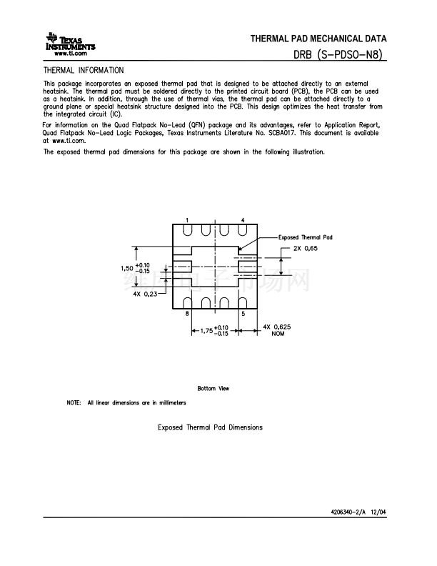
TPS736xx
www.ti.com
SBVS038K 鈥?SEPTEMBER 2003 鈥?REVISED SEPTEMBER 2005
This integrated circuit can be damaged by ESD. Texas Instruments recommends that all integrated
circuits be handled with appropriate precautions. Failure to observe proper handling and installation
procedures can cause damage.
ESD damage can range from subtle performance degradation to complete device failure. Precision
integrated circuits may be more susceptible to damage because very small parametric changes could
cause the device not to meet its published specifications.
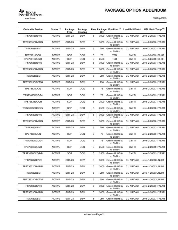
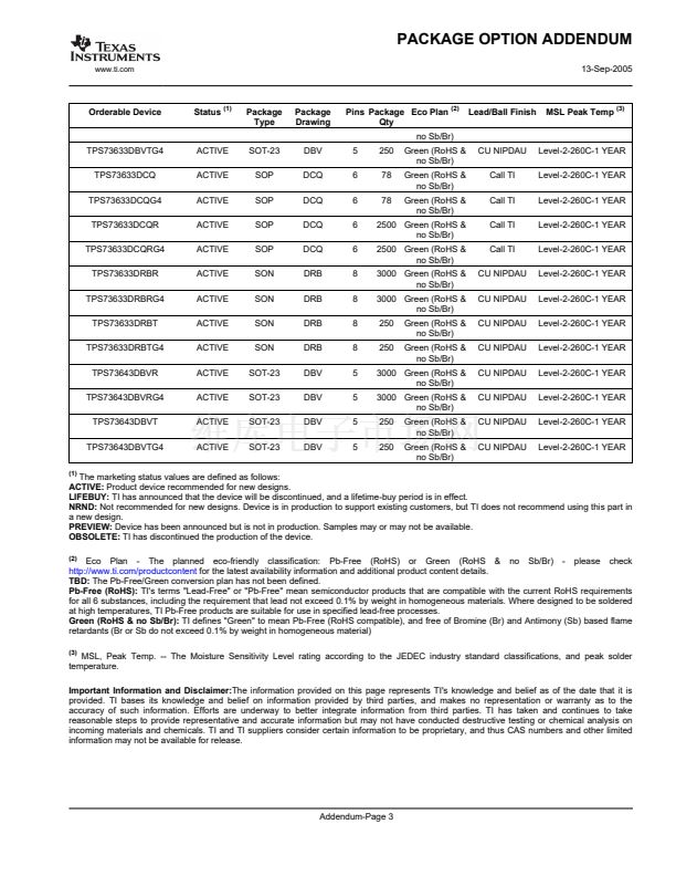
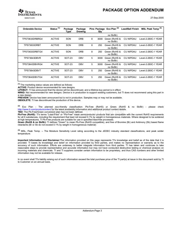
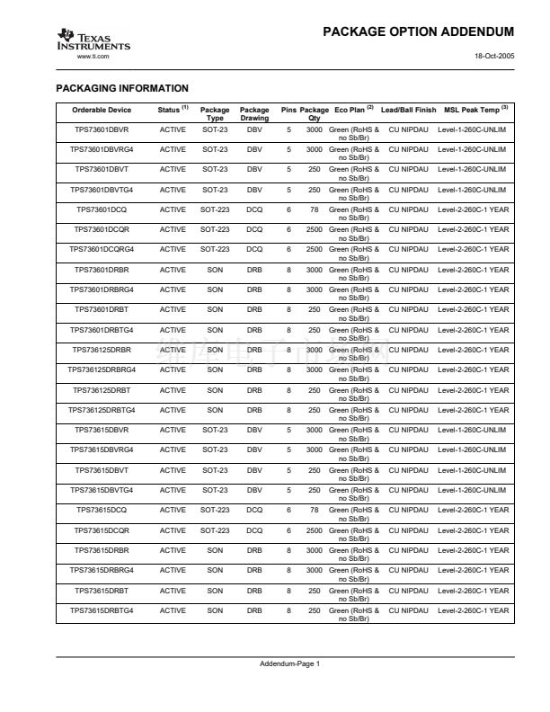
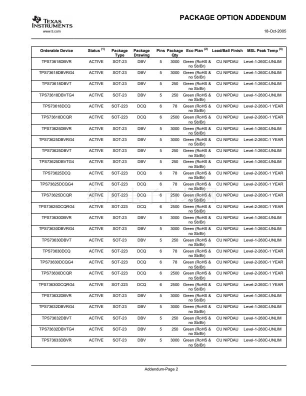
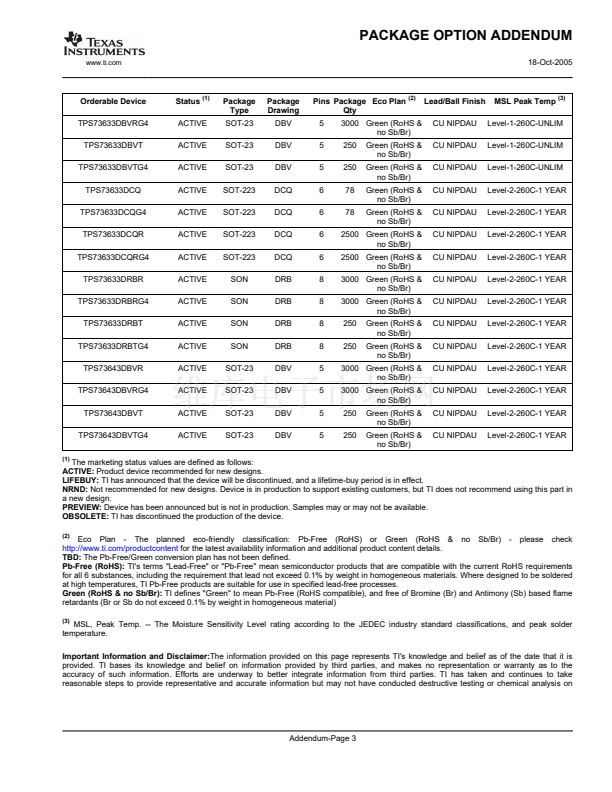
ORDERING INFORMATION
(1)
PRODUCT
TPS736xxyyyz
V
OUT (2)
XX
is nominal output voltage (for example, 25 = 2.5V, 01 = Adjustable
(3)
).
YYY
is package designator.
Z
is package quantity.
(1)
(2)
(3)
For the most current specification and package information, refer to the Package Option Addendum located at the end of this datasheet
or see the TI website at
www.ti.com.
Additional output voltages from 1.25V to 4.3V in 100mV increments are available on a quick-turn basis using innovative factory
EEPROM programming. Minimum order quantities apply; contact factory for details and availability.
For fixed 1.2V operation, tie FB to OUT.
ABSOLUTE MAXIMUM RATINGS
over operating free-air temperature range unless otherwise noted
(1)
TPS736xx
V
IN
range
V
EN
range
V
OUT
range
Peak output current
Output short-circuit duration
Continuous total power dissipation
Junction temperature range, T
J
Storage temperature range
ESD rating, HBM
ESD rating, CDM
(1)
-0.3 to 6.0
-0.3 to 6.0
-0.3 to 5.5
Internally limited
Indefinite
See
Dissipation Ratings Table
-55 to +150
-65 to +150
2
500
掳C
掳C
kV
V
UNIT
V
V
V
Stresses beyond those listed under Absolute Maximum Ratings may cause permanent damage to the device. These are stress ratings
only, and functional operation of the device at these or any other conditions beyond those indicated under the Electrical Characteristics
is not implied. Exposure to absolute maximum rated conditions for extended periods may affect device reliability.
POWER DISSIPATION RATINGS
(1)
BOARD
Low-K
(2)
High-K
(3)
Low-K
(2)
High-K
(3) (4)
(1)
(2)
(3)
(4)
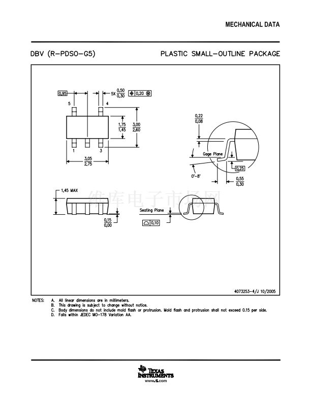
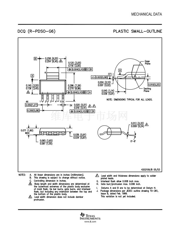
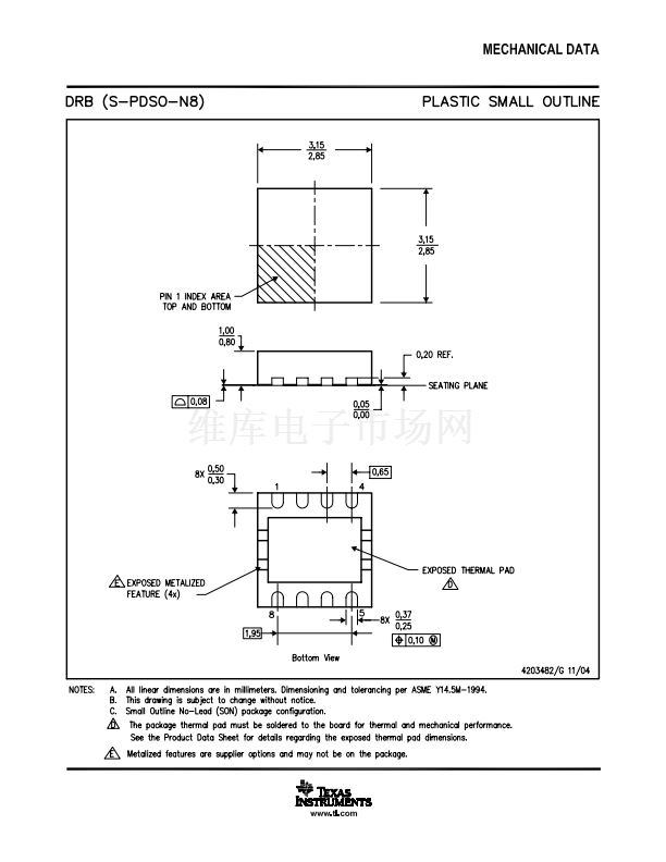
PACKAGE
DBV
DBV
DCQ
DRB
R
螛JC
64掳C/W
64掳C/W
15掳C/W
1.2掳C/W
R
螛JA
255掳C/W
180掳C/W
53掳C/W
40掳C/W
DERATING FACTOR
ABOVE T
A
= 25掳C
3.9mW/掳C
5.6mW/掳C
18.9mW/掳C
25.0mW/掳C
T
A
鈮?/div>
25掳C
POWER RATING
390mW
560mW
1.89W
2.50W
T
A
= 70掳C
POWER RATING
215mW
310mW
1.04W
1.38W
T
A
= 85掳C
POWER RATING
155mW
225mW
0.76W
1.0W
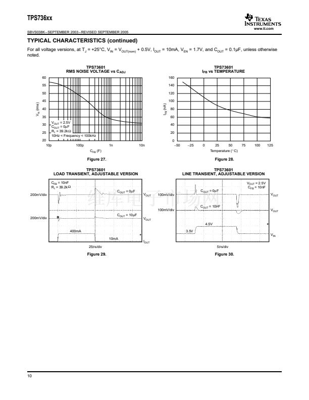
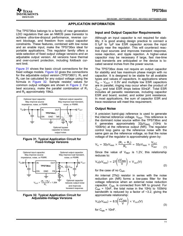
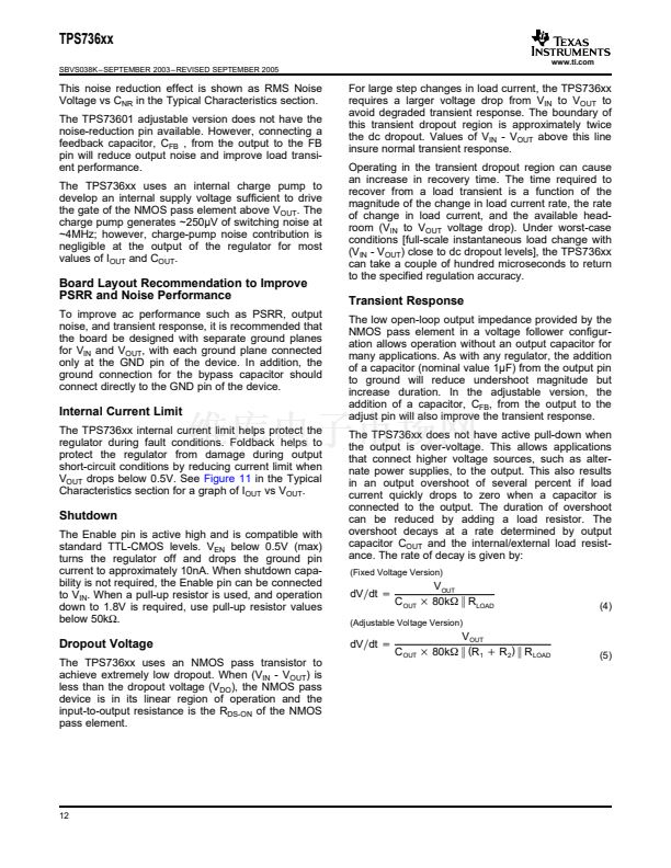
See
Power Dissipation
in the
Applications
section for more information related to thermal design.
The JEDEC Low-K (1s) board design used to derive this data was a 3inch x 3inch, 2-layer board with 2-ounce copper traces on top of
the board.
The JEDEC High-K (2s2p) board design used to derive this data was a 3inch x 3inch, multilayer board with 1-ounce internal power and
ground planes and 2-ounce copper traces on the top and bottom of the board.
Based on preliminary thermal simulations.
2


 1
1
 2
2
 3
3
 4
4
 5
5
 6
6
 7
7
 8
8
 9
9
 10
10
 11
11
 12
12
 13
13
 14
14
 15
15
 16
16
 17
17
 18
18
 19
19
 20
20
 21
21
 22
22
 23
23
 24
24
 25
25
 26
26
 27
27
