鈩?/div>
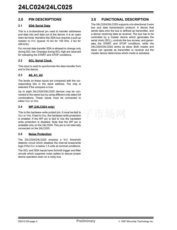
Serial EEPROM
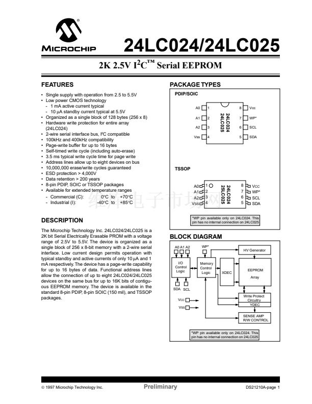
PACKAGE TYPES
PDIP/SOIC
A0
A1
A2
Vss
1
8
Vcc
WP*
SCL
SDA
鈥?Single supply with operation from 2.5 to 5.5V
鈥?Low power CMOS technology
- 1 mA active current typical
- 10
碌
A standby current typical at 5.5V
鈥?Organized as a single block of 128 bytes (256 x 8)
鈥?Hardware write protection for entire array
(24LC024)
鈥?2-wire serial interface bus, I
2
C compatible
鈥?100kHz and 400kHz compatibility
鈥?Page-write buffer for up to 16 bytes
鈥?Self-timed write cycle (including auto-erase)
鈥?3.5 ms typical write cycle time for page write
鈥?Address lines allow up to eight devices on bus
鈥?10,000,000 erase/write cycles guaranteed
鈥?ESD protection > 4,000V
鈥?Data retention > 200 years
鈥?8-pin PDIP, SOIC or TSSOP packages
鈥?Available for extended temperature ranges
- Commercial (C):
0
掳
C to +70
掳
C
- Industrial (I):
-40
掳
C to +85
掳
C
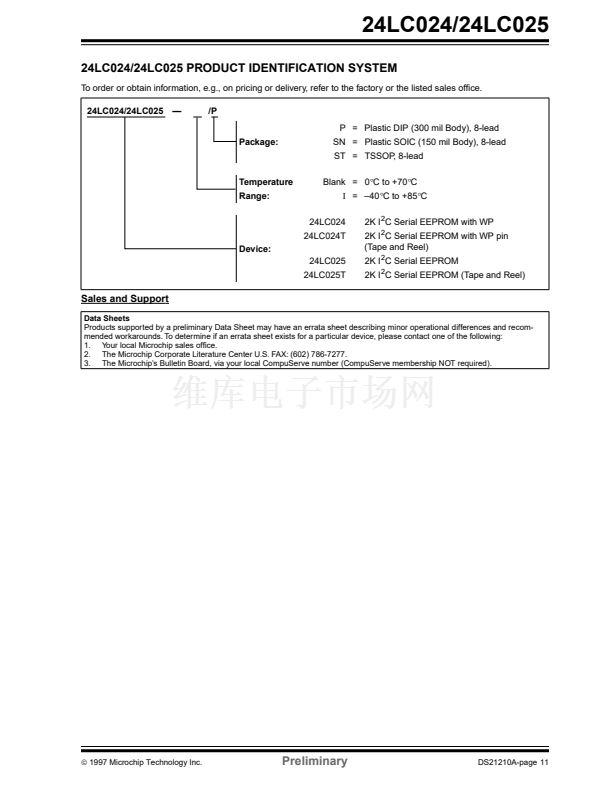
24LC024
24LC025
2
3
4
7
6
5
TSSOP
A0
A1
A2
V
SS
1
2
3
4
8
7
6
5
V
CC
WP*
SCL
SDA
DESCRIPTION
The Microchip Technology Inc. 24LC024/24LC025 is a
2K bit Serial Electrically Erasable PROM with a voltage
range of 2.5V to 5.5V. The device is organized as a
single block of 256 x 8-bit memory with a 2-wire serial
interface. Low current design permits operation with
typical standby and active currents of only 10
碌
A and 1
mA respectively. The device has a page-write capability
for up to 16 bytes of data. Functional address lines
allow the connection of up to eight 24LC024/24LC025
devices on the same bus for up to 16K bits of contigu-
ous EEPROM memory. The device is available in the
standard 8-pin PDIP, 8-pin SOIC (150 mil), and TSSOP
packages.
*WP pin available only on 24LC024. This
pin has no internal connection on 24LC025
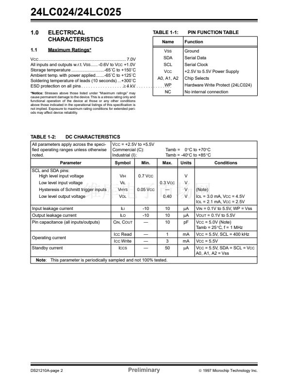
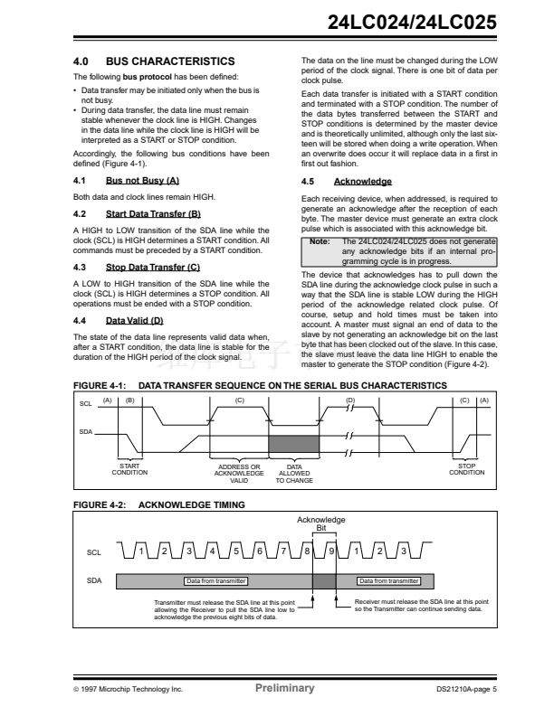
BLOCK DIAGRAM
A0 A1 A2
WP*
HV Generator
24LC024
25LC025
I/O
Control
Logic
Memory
Control
Logic
XDEC
EEPROM
Array
SDA SCL
V
CC
V
SS
Write Protect
Circuitry
YDEC
SENSE AMP
R/W CONTROL
*WP pin available only on 24LC024. This
pin has no internal connection on 24LC025
漏
1997 Microchip Technology Inc.
Preliminary
DS21210A-page 1


 1
1
 2
2
 3
3
 4
4
 5
5
 6
6
 7
7
 8
8
 9
9
 10
10
 11
11
 12
12
