鈩?/div>
compatible
鈥?Self-timed write cycle (including auto-erase)
鈥?Page-write buffer for up to 8 bytes
鈥?100 kHz (2.5V) and 400 kHz (5V) compatibility
鈥?Factory programming (QTP) available
鈥?1,000,000 erase/write cycles guaranteed
鈥?Data retention > 200 years
鈥?8-pin PDIP and SOIC package
鈥?Available for extended temperature ranges
- Commercial (C):
0藲C to +70藲C
- Industrial (I):
-40藲C to +85藲C
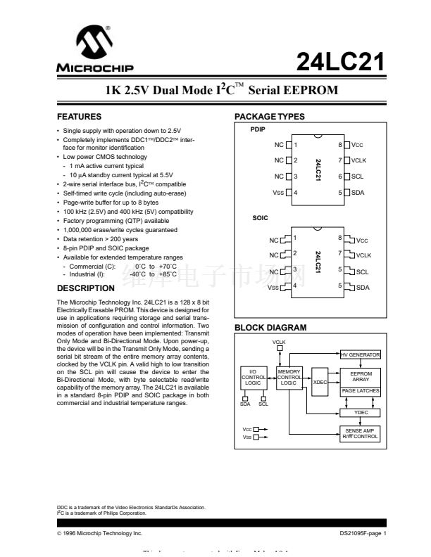
PACKAGE TYPES
PDIP
NC
NC
NC
V
SS
1
2
3
4
24LC21
8
7
6
5
V
CC
VCLK
SCL
SDA
SOIC
1
2
3
4
24LC21
8
7
5
5
NC
NC
NC
V
SS
V
CC
VCLK
SCL
SDA
DESCRIPTION
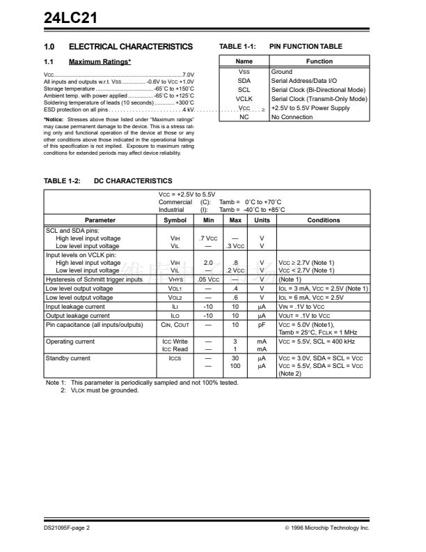
The Microchip Technology Inc. 24LC21 is a 128 x 8 bit
Electrically Erasable PROM. This device is designed for
use in applications requiring storage and serial trans-
mission of con铿乬uration and control information. Two
modes of operation have been implemented: Transmit
Only Mode and Bi-Directional Mode. Upon power-up,
the device will be in the Transmit Only Mode, sending a
serial bit stream of the entire memory array contents,
clocked by the VCLK pin. A valid high to low transition
on the SCL pin will cause the device to enter the
Bi-Directional Mode, with byte selectable read/write
capability of the memory array. The 24LC21 is available
in a standard 8-pin PDIP and SOIC package in both
commercial and industrial temperature ranges.
BLOCK DIAGRAM
VCLK
HV GENERATOR
I/O
CONTROL
LOGIC
MEMORY
CONTROL
LOGIC
XDEC
EEPROM
ARRAY
PAGE LATCHES
SDA
SCL
YDEC
V
CC
V
SS
SENSE AMP
R/W CONTROL
DDC is a trademark of the Video Electronics StandarDs Association.
I
2
C is a trademark of Philips Corporation.
漏
1996 Microchip Technology Inc.
DS21095F-page 1
This document was created with FrameMaker 4 0 4


 1
1
 2
2
 3
3
 4
4
 5
5
 6
6
 7
7
 8
8
 9
9
 10
10
 11
11
 12
12
