鈥?/div>
LNA 2
+
VPS2
3
CLAMP
03199-B-001
COM2
6
4
5
7
8
14
18
11
LON2
LOP2
VIP2
VIN2
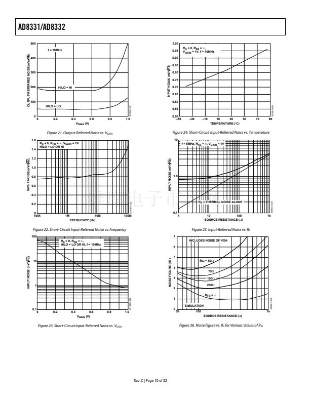
APPLICATIONS
50
Figure 1. AD8332 Shown 28-Lead TSSOP
V
GAIN
= 1V
40
0.8V
30
0.6V
20
0.4V
10
0.2V
0
鈥?0
鈥?0
100k
0V
Ultrasound and sonar time-gain control
High performance AGC systems
I/Q signal processing
High speed dual ADC driver
GENERAL DESCRIPTION
The AD8331/AD8332 are single- and dual-channel ultralow
noise, linear-in-dB, variable gain amplifiers. Although optimized
for ultrasound systems, they are usable as low noise variable
gain elements at frequencies up to 120 MHz.
Each channel consists of an ultralow noise preamplifier (LNA),
an X-AMP庐 VGA with 48 dB of gain range, and a selectable gain
postamplifier with adjustable output limiting. The LNA gain is
19 dB with a single-ended input and differential outputs capable
of accurate, programmable active input impedance matching by
selecting an external feedback resistor. Active impedance
control optimizes noise performance for applications that
benefit from input matching.
The 48 dB gain range of the VGA makes these devices suitable
for a variety of applications. Excellent bandwidth uniformity is
maintained across the entire range. The gain control interface
provides precise linear-in-dB scaling of 50 dB/V for control
voltages between 40 mV and 1 V. Factory trim ensures excellent
part-to-part and channel-to-channel gain matching. Differential
signal paths lead to superb second and third order distortion
performance and low crosstalk.
GAIN (dB)
1M
10M
FREQUENCY (Hz)
100M
1G
Figure 2. Frequency Response vs. Gain
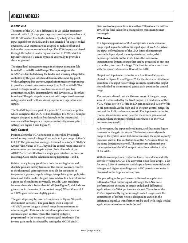
The VGA鈥檚 low output-referred noise is advantageous in driving
high speed differential ADCs. The gain of the postamplifier may
be pin selected to 3.5 dB or 15.5 dB to optimize gain range and
output noise for 12-bit or 10-bit converter applications. The
output may be limited to a user-selected clamping level,
preventing input overload to a subsequent ADC. An external
resistor adjusts the clamping level.
The operating temperature range is 鈥?0掳C to +85掳. The
AD8331 is available in a 20-lead QSOP package, and the
AD8332 in 28-lead TSSOP and 32-lead LFCSP packages. They
require a single 5 V supply, and the quiescent power
consumption is 125 mW/ch. A power-down (enable) pin is
provided.
Rev. C
Information furnished by Analog Devices is believed to be accurate and reliable.
However, no responsibility is assumed by Analog Devices for its use, nor for any
infringements of patents or other rights of third parties that may result from its use.
Specifications subject to change without notice. No license is granted by implication
or otherwise under any patent or patent rights of Analog Devices. Trademarks and
registered trademarks are the property of their respective owners.
One Technology Way, P.O. Box 9106, Norwood, MA 02062-9106, U.S.A.
Tel: 781.329.4700
www.analog.com
Fax: 781.326.8703
漏 2003 Analog Devices, Inc. All rights reserved.
03199-C-002
+
VGA 2
鈥?/div>
POST
AMP2
COMM
ENB
RCLMP
13
VOL2
12
VOH2


 1
1
 2
2
 3
3
 4
4
 5
5
 6
6
 7
7
 8
8
 9
9
 10
10
 11
11
 12
12
 13
13
 14
14
 15
15
 16
16
 17
17
 18
18
 19
19
 20
20
 21
21
 22
22
 23
23
 24
24
 25
25
 26
26
 27
27
 28
28
 29
29
 30
30
 31
31
 32
32
