鈥?Pin-compatible and functionally equivalent to ZBT鈩?/div>
鈥?Supports 250-MHz bus operations with zero wait states
鈥?Available speed grades are 250, 200 and 167 MHz
鈥?Internally self-timed output buffer control to eliminate the
need to use asynchronous OE
鈥?Fully registered (inputs and outputs) for pipelined
operation
鈥?Byte Write capability
鈥?Single 3.3V power supply
鈥?3.3V/2.5V I/O power supply
鈥?Fast clock-to-output times
鈥?2.6 ns (for 250-MHz device)
鈥?3.2 ns (for 200-MHz device)
鈥?3.4 ns (for 167-MHz device)
鈥?Clock Enable (CEN) pin to suspend operation
鈥?Synchronous self-timed writes
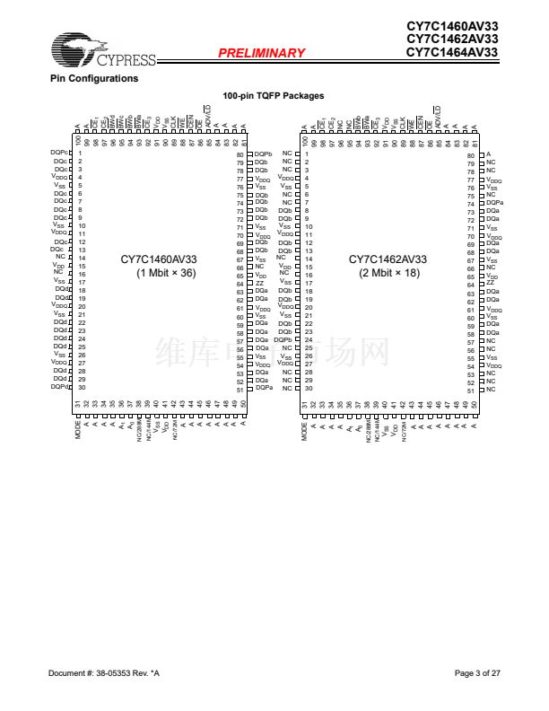
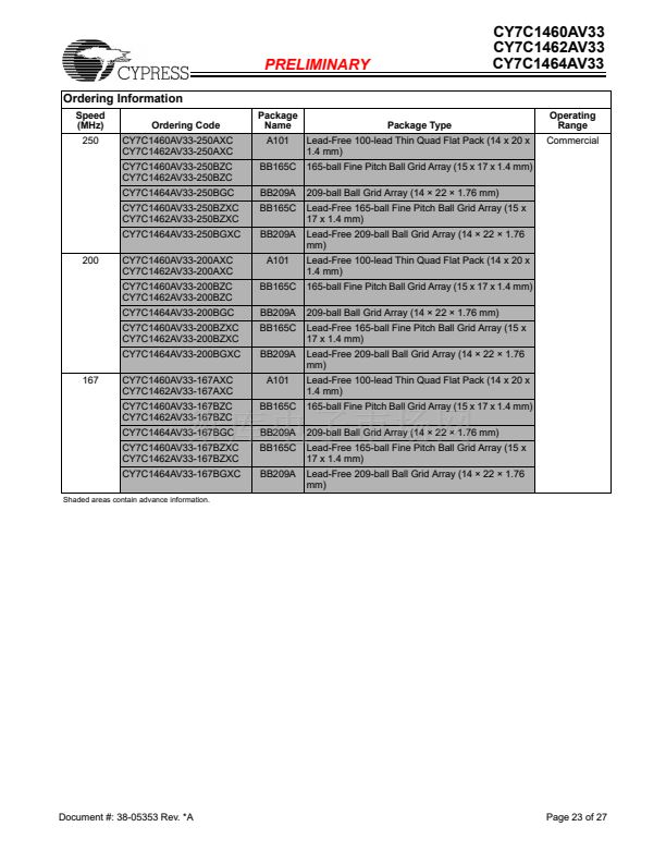
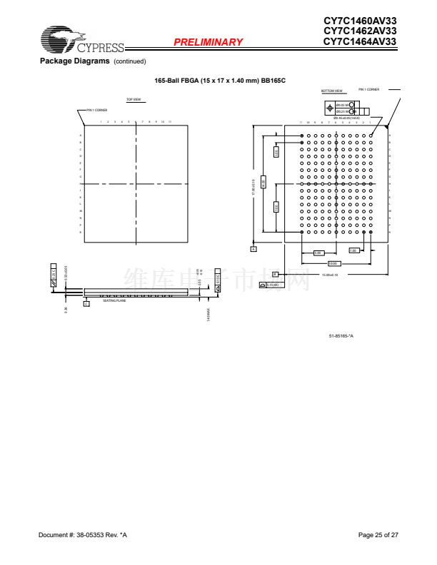
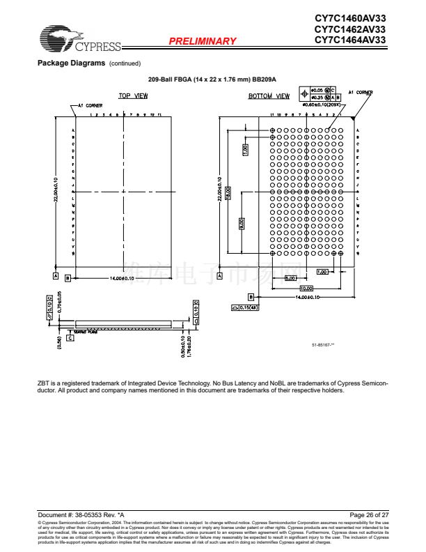
鈥?CY7C1460AV33 and CY7C1462AV33 are available in
lead-free 100-pin TQFP and 165-Ball fBGA packages;
CY7C1464AV33 available in 209-Ball fBGA package
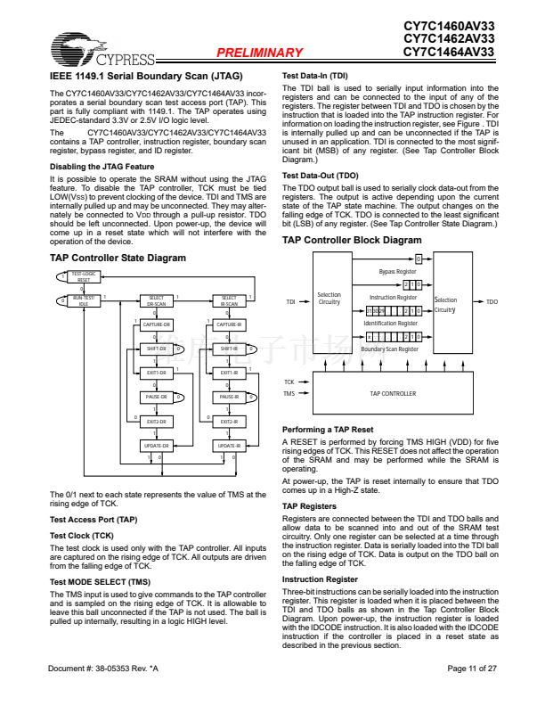
鈥?IEEE 1149.1 JTAG Boundary Scan
鈥?Burst capability鈥攍inear or interleaved burst order
鈥?鈥淶Z鈥?Sleep Mode option and Stop Clock option
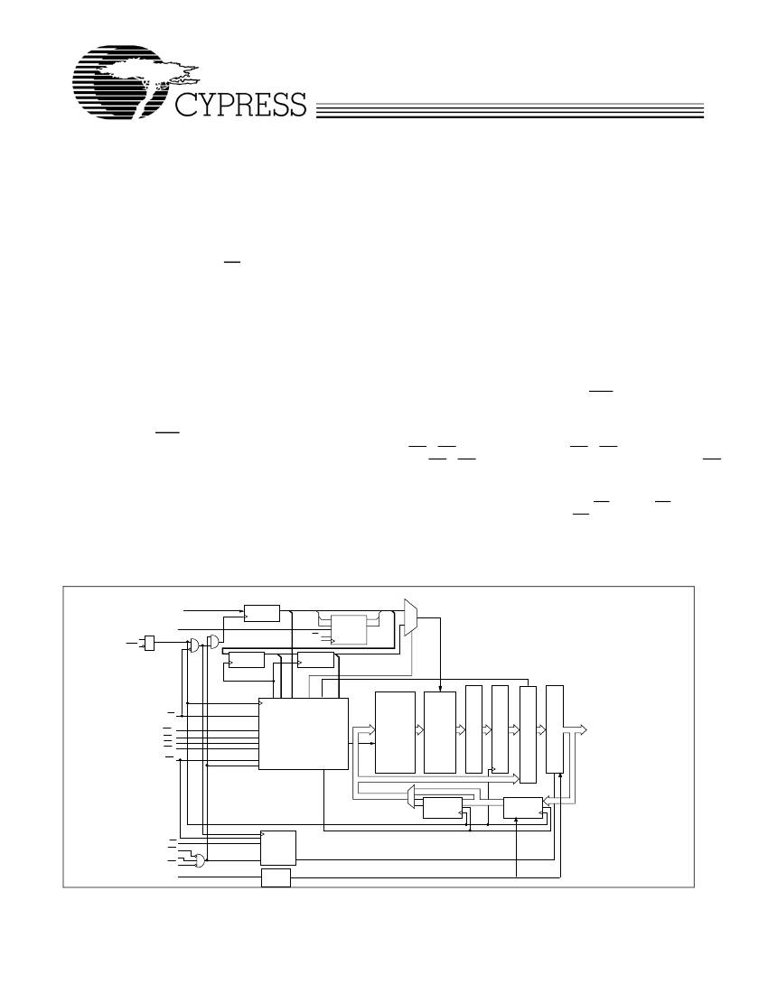
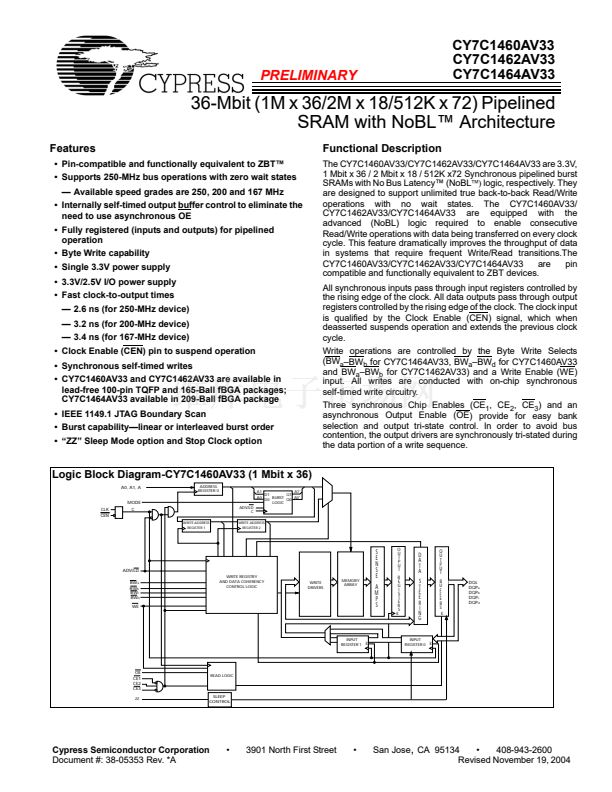
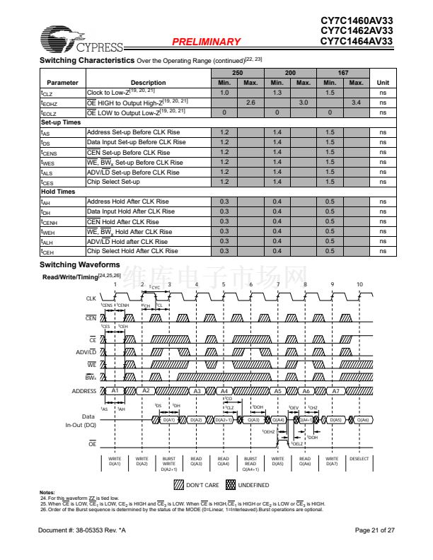
Functional Description
The CY7C1460AV33/CY7C1462AV33/CY7C1464AV33 are 3.3V,
1 Mbit x 36 / 2 Mbit x 18 / 512K x72 Synchronous pipelined burst
SRAMs with No Bus Latency鈩?(NoBL鈩? logic, respectively. They
are designed to support unlimited true back-to-back Read/Write
operations with no wait states. The CY7C1460AV33/
CY7C1462AV33/CY7C1464AV33 are equipped with the
advanced (NoBL) logic required to enable consecutive
Read/Write operations with data being transferred on every clock
cycle. This feature dramatically improves the throughput of data
in systems that require frequent Write/Read transitions.The
CY7C1460AV33/CY7C1462AV33/CY7C1464AV33
are
pin
compatible and functionally equivalent to ZBT devices.
All synchronous inputs pass through input registers controlled by
the rising edge of the clock. All data outputs pass through output
registers controlled by the rising edge of the clock. The clock input
is qualified by the Clock Enable (CEN) signal, which when
deasserted suspends operation and extends the previous clock
cycle.
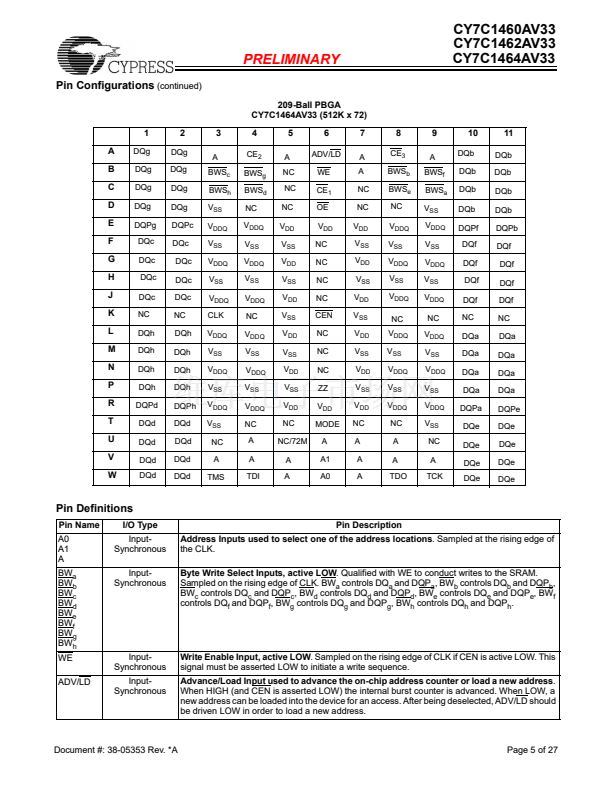
Write operations are controlled by the Byte Write Selects
(BW
a
鈥揃W
h
for CY7C1464AV33, BW
a
鈥揃W
d
for CY7C1460AV33
and BW
a
鈥揃W
b
for CY7C1462AV33) and a Write Enable (WE)
input. All writes are conducted with on-chip synchronous
self-timed write circuitry.
Three synchronous Chip Enables (CE
1
, CE
2
, CE
3
) and an
asynchronous Output Enable (OE) provide for easy bank
selection and output tri-state control. In order to avoid bus
contention, the output drivers are synchronously tri-stated during
the data portion of a write sequence.
Logic Block Diagram-CY7C1460AV33 (1 Mbit x 36)
A0, A1, A
MODE
CLK
CEN
ADDRESS
REGISTER 0
A1
A1'
D1
Q1
A0
A0'
BURST
D0
Q0
LOGIC
ADV/LD
C
WRITE ADDRESS
REGISTER 1
WRITE ADDRESS
REGISTER 2
C
ADV/LD
BW
a
BW
b
BW
c
BW
d
WE
WRITE REGISTRY
AND DATA COHERENCY
CONTROL LOGIC
WRITE
DRIVERS
MEMORY
ARRAY
S
E
N
S
E
A
M
P
S
O
U
T
P
U
T
R
E
G
I
S
T
E
R
S
D
A
T
A
S
T
E
E
R
I
N
G
O
U
T
P
U
T
B
U
F
F
E
R
S
E
DQs
DQP
a
DQP
b
DQP
c
DQP
d
E
INPUT
REGISTER 1
E
INPUT
REGISTER 0
E
OE
CE1
CE2
CE3
ZZ
READ LOGIC
SLEEP
CONTROL
Cypress Semiconductor Corporation
Document #: 38-05353 Rev. *A
鈥?/div>
3901 North First Street
鈥?/div>
San Jose
,
CA 95134
鈥?/div>
408-943-2600
Revised November 19, 2004


 1
1
 2
2
 3
3
 4
4
 5
5
 6
6
 7
7
 8
8
 9
9
 10
10
 11
11
 12
12
 13
13
 14
14
 15
15
 16
16
 17
17
 18
18
 19
19
 20
20
 21
21
 22
22
 23
23
 24
24
 25
25
 26
26
 27
27
